LH530800A
LH530800A is CMOS 1M (128K x 8) MROM manufactured by Sharp Corporation.
FEATURES
- 131,072 words × 8 bit organization
- Access time: 150 ns (MAX.)
- Power consumption: Operating: 192.5 m W (MAX.) Standby: 550 µW (MAX.)
- Static operation
- TTL patible I/O
- Three-state outputs
- Single +5 V power supply
- Packages: 32-pin, 600-mil DIP 32-pin, 525-mil SOP 32-pin, 450-mil QFJ (PLCC)
- JEDEC standard EPROM pinout (DIP) DESCRIPTION
The LH530800A is a mask-programmable ROM organized as 131,072 × 8 bits (1,048,576 bits). It is fabricated using silicon-gate CMOS process technology.
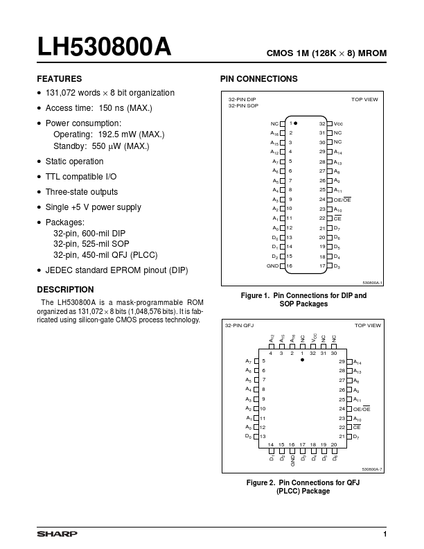
32-PIN DIP 32-PIN SOP
CMOS 1M (128K × 8) MROM
PIN CONNECTIONS
TOP VIEW
NC A16 A15 A12 A7 A6 A5 A4 A3 A2 A1 A0 D0 D1 D2 GND
1 2 3 4 5 6 7 8 9 10 11 12 13 14 15 16
32 31 30 29 28 27 26 25 24 23 22 21 20 19 18 17
Vcc NC NC A14 A13 A8 A9 A11 OE/OE A10 CE D7 D6 D5 D4 D3
530800A-1
Figure 1. Pin Connections for DIP and SOP Packages
32-PIN QFJ TOP VIEW
A12
A15
A16
4 A7 A6 A5 A4 A3 A2 A1 A0 D0 5 6 7 8 9 10 11 12 13
32 31 30 29 28 27 26 25 24 23 22 21 A14 A13 A8 A9 A11 OE/OE A10 CE D7
14 15 16 17 18 19 20
D1
D2
D3
D4
D5...