J425
monolithic dual
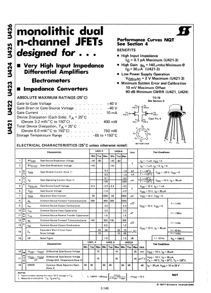
H n-channel JFETs Performance Curves NQT See Sedion 4 designed for
- -
- - Very High Input Impedance Di Herential Amplifiers
Electrometers
- Impedance Converters
BENEFITS
- High Input Impedance IG = 0.1 p A Maximum (U421-3)
- High Gain gfs = 140 !,mho Minimum@ ID= 3O I'A (U421- 3)
- Low Power Supply Operation VGS(off) = 2 V Maximum (U421- 3)
- Minimum System Error and Calibration 10 m V Maximum Offset
90 d B Minimum CMRR (U421, U424)
ABSOLUTE MAXIMUM RATINGS (25°C)
TO- 78
See Section 5
Gate-to-Gate Voltage Gate-Drain or Gate-Source Voltage Gate Current Device Dissipation (Each Side), TA = 25°C
(Derate 3.2 m W;o C to 150°C) .
- Total Device Dissipation, TA = 25°C
! (Derate 6.0 m W;o C to 150°C) Storage Temperature Range
±40 V -40 V 10m A
400m W
750 m W -65 to +150°C
~G,
Pf N3
5,
D,
PIN 6
G, PIN 7
5, Case Pin 4
PIN 1
PIN 5
5, c
4 a S D2 o~ G1 300
G2
'0 '
5, 01 10
A '2
~,
G,
ELECTRICAL CHARACTERISTICS (25°C unless otherwise...