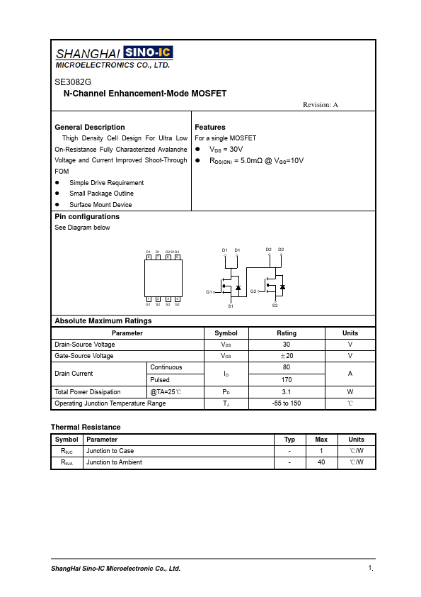
Datasheet4U Logo Datasheet4U.com

SE3082G - N-Channel MOSFET

Download the SE3082G datasheet PDF. This datasheet also covers the SE3082G-Sino variant, as both devices belong to the same n-channel mosfet family and are provided as variant models within a single manufacturer datasheet.

General Description

Thigh Density Cell Design For Ultra Low On-Resistance Fully Characterized Avalanche Voltage and Current Improved Shoot-Through FOM Simple Drive Requirement Small Package Outline Surface Mount Device

Key Features

  • For a single MOSFET.
  • VDS = 30V.
  • RDS(ON) = 5.0mΩ @ VGS=10V Pin configurations See Diagram below D1 D1 D2 S1D2 87 65 D1 D1 D2 D2 1 2 34 G1 S2 S2 G2 Absolute Maximum Ratings Parameter Drain-Source Voltage Gate-Source Voltage Drain Current Continuous Pulsed Total Power Dissipation @TA=25℃ Operating Junction Temperature Range Thermal Resistance Symbol RθJC RθJA Parameter Junction to Case Junction to Ambient G1 S1 G2 S2 Symbol VDS VGS ID PD TJ Rating 30 ±20 80 170 3.1 -5.

📥 Download Datasheet

Note: The manufacturer provides a single datasheet file (SE3082G-Sino-IC.pdf) that lists specifications for multiple related part numbers.

Datasheet Details

Part number SE3082G
Manufacturer Sino-IC
File Size 590.23 KB
Description N-Channel MOSFET
Datasheet download datasheet SE3082G Datasheet

Full PDF Text Transcription (Reference)

The following content is an automatically extracted verbatim text from the original manufacturer datasheet and is provided for reference purposes only.

View original datasheet text
SE3082G N-Channel Enhancement-Mode MOSFET Revision: A General Description Thigh Density Cell Design For Ultra Low On-Resistance Fully Characterized Avalanche Voltage and Current Improved Shoot-Through FOM  Simple Drive Requirement  Small Package Outline  Surface Mount Device Features For a single MOSFET  VDS = 30V  RDS(ON) = 5.0mΩ @ VGS=10V Pin configurations See Diagram below D1 D1 D2 S1D2 87 65 D1 D1 D2 D2 1 2 34 G1 S2 S2 G2 Absolute Maximum Ratings Parameter Drain-Source Voltage Gate-Source Voltage Drain Current Continuous Pulsed Total Power Dissipation @TA=25℃ Operating Junction Temperature Range Thermal Resistance Symbol RθJC RθJA Parameter Junction to Case Junction to Ambient G1 S1 G2 S2 Symbol VDS VGS ID PD TJ Rating 30 ±20 80 170 3.