• Part: ST3413A
  • Description: MOSFET
  • Category: MOSFET
  • Manufacturer: Stanson Technology
  • Size: 258.66 KB
Download ST3413A Datasheet PDF
Stanson Technology
ST3413A
ST3413A is MOSFET manufactured by Stanson Technology.
DESCRIPTION 
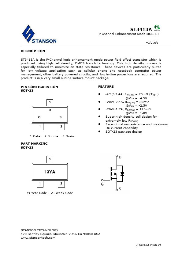
ST3413A is the P-Channel logic enhancement mode power field effect transistor which is produced using high cell density, DMOS trench technology. This high density process is especially tailored to minimize on-state resistance. These devices are particularly suited for low voltage application such as cellular phone and notebook puter power management, other battery powered circuits, and low in-line power loss are required. The product is in a very small outline surface mount package. PIN CONFIGURATION SOT-23 3 D GS 1.Gate 2.Source 3.Drain PART MARKING SOT-23 FEATURE -20V/-3.4A, RDS(ON) = 70mΩ (Typ.) @VGS = -4.5V -20V/-2.4A, RDS(ON) = 80mΩ @VGS = -2.5V -20V/-1.7A, RDS(ON) = 125mΩ @VGS = -1.8V Super high density cell design for extremely low RDS(ON) Exceptional on-resistance and maximum DC current capability SOT-23 package design 13YA 12 Y: Year Code A: Week Code STANSON TECHNOLOGY 120 Bentley Square, Mountain View, Ca 94040 USA .stansontech. ST3413A 2006 V1 P Channel Enhancement Mode MOSFET -3.5A ABSOULTE MAXIMUM RATINGS (Ta = 25℃ Unless otherwise noted ) Parameter Symbol Typical Drain-Source Voltage Gate-Source Voltage Continuous Drain Current (TJ=150℃) Pulsed Drain Current TA=25℃ TA=70℃ VDSS VGSS ID IDM -20 ±8 -3.5 -2.8 -15 Continuous Source Current (Diode Conduction) Power Dissipation TA=25℃ TA=70℃ Operation Junction Temperature IS -1.4 1.25 0.8 TJ -55/150 Storage Temperature Range TSTG -55/150 Thermal Resistance-Junction to...