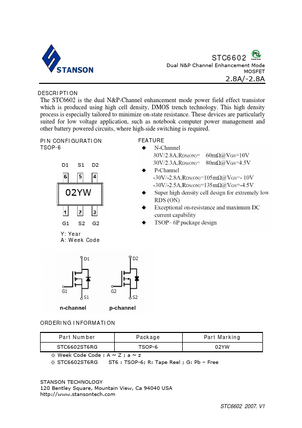
DESCRIPTION
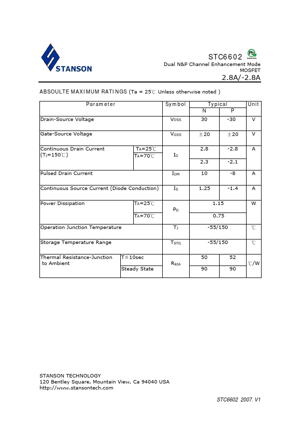
PIN CONFIGURATION TSOP-6 FEATURE D1 S1 D2 02YW G1 S2 G2 Y: Year A: Week Code ORDERING INFORMATION Part Number Package Part Marking STC6602ST6RG TSOP-6 02YW ※ Week Code Code : A ~ Z ; a ~ z ※ STC6602ST6RG ST6 : TSOP-6; R: Tape Reel ; G: Pb – Free STANSON TECHNOLOGY 120 Bentley Square, Mountain View, Ca 94040 USA STC6602 2007. V1 STC6602 Dual N&P Channel Enhancement Mode MOSFET 2.8A/-2.8A ABSOULTE MAXIMUM RATINGS
(Ta = 25℃ Unless otherwise noted ) Parameter Drain-Source Voltage Symbol VDSS Typical NP 30 -30 Unit V Gate-Source Voltage VGSS ±20 ±20 V Continuous Drain Current (TJ=150℃) Pulsed Drain Current TA=25℃ TA=70℃ ID IDM 2.8 -2.8 A 2.3 -2.1 10 -8 A Continuous Source Current (Diode Conduction) IS 1.25 -1.4 A Power Dissipation Operation Junction Temperature TA=25℃ TA=70℃ PD TJ 1.15 0.75 -55/150 W ℃ Storage Temperature Range TSTG -55/150 ℃ Thermal Resistance-Junction to Ambient T≦10sec Steady State RθJA 50 90 52 ℃/W 90 STANSON TECHNOLOGY 120 Bentley Square, Mountain View, Ca 94040 USA STC6602 2007. Stanson Technology