2SK3842
2SK3842 is N-Channel MOSFET manufactured by Toshiba.
TOSHIBA Field Effect Transistor Silicon N Channel MOS Type (U-MOSIII)
Switching Regulator Applications, DC-DC Converter and Motor Drive Applications
- -
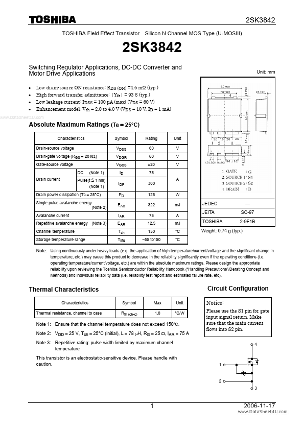
- - Low drain-source ON resistance: RDS (ON) =4.6 mΩ (typ.) High forward transfer admittance: |Yfs| = 93 S (typ.) Low leakage current: IDSS = 100 μA (max) (VDS = 60 V) Enhancement model: Vth = 2.0 to 4.0 V (VDS = 10 V, ID = 1 m A) Unit: mm
..
Absolute Maximum Ratings (Ta = 25°C)
Characteristics Drain-source voltage Drain-gate voltage (RGS = 20 kΩ) Gate-source voltage DC Drain current (Note 1) (Note 1) Drain power dissipation (Tc = 25°C) Single pulse avalanche energy (Note 2) Avalanche current Repetitive avalanche energy (Note 3) Channel temperature Storage temperature range Pulse(t < = 1 ms) Symbol VDSS VDGR VGSS ID IDP PD EAS IAR EAR Tch Tstg Rating 60 60 ±20 75 300 125 322 75 12.5 150
- 55 to150 A Unit V V V
W m J A m J °C °C
JEDEC JEITA TOSHIBA
― SC-97 2-9F1B
Weight: 0.74 g (typ.)
Note: Using continuously under heavy loads (e.g. the application of high temperature/current/voltage and the significant change in temperature, etc.) may cause this product to decrease in the reliability significantly even if the operating conditions (i.e. operating temperature/current/voltage, etc.) are within the absolute maximum ratings. Please design the appropriate reliability upon reviewing the Toshiba Semiconductor Reliability Handbook (“Handling Precautions”/Derating Concept and Methods) and individual reliability data (i.e. reliability test report and estimated failure rate, etc).
Thermal Characteristics
Characteristics Thermal resistance, channel to case Symbol Rth (ch-c) Max 1.0 Unit °C/W
Circuit Configuration
Notice:
Please use the S1 pin for gate input signal return. Make sure that the main current flows into S2 pin.
Note 1: Ensure that the channel temperature does not exceed 150℃. Note 2: VDD = 25 V, Tch = 25°C (initial), L = 78 μH, RG = 25 Ω, IAR = 75 A Note 3: Repetitive rating: pulse width...