SSM3J01T
SSM3J01T is TOSHIBA Field Effect Transistor Silicon P Channel MOS Type manufactured by Toshiba.
TOSHIBA Field Effect Transistor Silicon P Channel MOS Type
Power Management Switch High Speed Switching Applications
- -
- Small Package Low on Resistance : Ron = 0.4 Ω (max) (@VGS =
- 4 V) : Ron = 0.6 Ω (max) (@VGS =
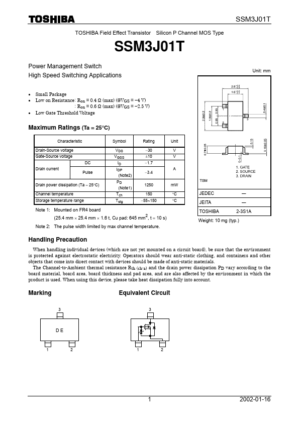
- 2.5 V) Low Gate Threshold Voltage Unit: mm
Maximum Ratings (Ta = 25°C)
Characteristic Drain-Source voltage Gate-Source voltage DC Drain current Pulse Symbol VDS VGSS ID IDP (Note2) PD (Note1) Tch Tstg Rating -30 ±10 -1.7 -3.4 1250 150 -55~150 2 A Unit V V
Drain power dissipation (Ta = 25°C) Channel temperature Storage temperature range m W °C °C
JEDEC JEITA TOSHIBA
― ― 2-3S1A
Note 1: Mounted on FR4 board (25.4 mm ´ 25.4 mm ´ 1.6 t, Cu pad: 645 mm , t = 10 s) Note 2: The pulse width limited by max channel temperature.
Weight: 10 mg (typ.)
Handling Precaution
When handling individual devices (which are not yet mounted on a circuit board), be sure that the environment is protected against electrostatic electricity. Operators should wear anti-static clothing, and containers and other objects that e into direct contact with devices should be made of anti-static materials. The Channel-to-Ambient thermal resistance Rth (ch-a) and the drain power dissipation PD vary according to the board material, board area, board thickness and pad area, and are also affected by the environment in which the product is used. When using this device, please take heat dissipation fully into account.
Marking
Equivalent Circuit
2002-01-16
Electrical Characteristics (Ta = 25°C)
Characteristic Gate leakage current Drain-Source breakdown voltage Drain Cut-off current Gate threshold voltage Forward transfer admittance Drain-Source ON resistance Drain-Source ON resistance Input capacitance Reverse transfer capacitance Output capacitance Switching time Turn-on time Turn-off time Symbol IGSS V (BR) DSS IDSS Vth |Yfs| RDS (ON) RDS (ON) Ciss Crss Coss ton toff Test Condition VGS = ±10 V, VDS = 0 ID = -1 m A, VGS = 0 VDS = -30 V,...