SSM3J02T
SSM3J02T is TOSHIBA Field Effect Transistor Silicon P Channel MOS Type manufactured by Toshiba.
TOSHIBA Field Effect Transistor Silicon P Channel MOS Type
Power Management Switch High Speed Switching Applications
- -
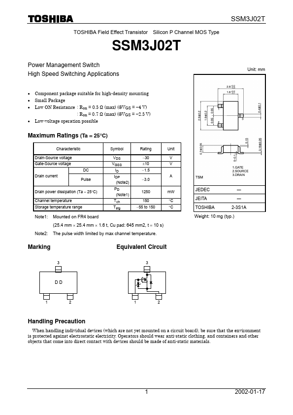
- - ponent package suitable for high-density mounting Small Package Low ON Resistance : Ron = 0.5 Ω (max) (@VGS =
- 4 V) : Ron = 0.7 Ω (max) (@VGS =
- 2.5 V) Low-voltage operation possible Unit: mm
Maximum Ratings (Ta = 25°C)
Characteristic Drain-Source voltage Gate-Source voltage DC Drain current Pulse Symbol VDS VGSS ID IDP (Note2) PD (Note1) Tch Tstg Rating -30 ±10 -1.5 -3.0 1250 150 -55 to 150 A Unit V V
Drain power dissipation (Ta = 25°C) Channel temperature Storage temperature range m W °C °C
JEDEC JEITA TOSHIBA
― ― 2-3S1A
Note1:
Mounted on FR4 board (25.4 mm ´ 25.4 mm ´ 1.6 t, Cu pad: 645 mm2, t = 10 s)
Weight: 10 mg (typ.)
Note2:
The pulse width limited by max channel temperature.
Marking
Equivalent Circuit
Handling Precaution
When handling individual devices (which are not yet mounted on a circuit board), be sure that the environment is protected against electrostatic electricity. Operators should wear anti-static clothing, and containers and other objects that e into direct contact with devices should be made of anti-static materials.
2002-01-17
Electrical Characteristics (Ta = 25°C)
Characteristic Gate leakage current Drain-Source breakdown voltage Drain Cut-off current Gate threshold voltage Forward transfer admittance Drain-Source ON resistance Input capacitance Reverse transfer capacitance Output capacitance Switching time Turn-on time Turn-off time Symbol IGSS V (BR) DSS IDSS Vth |Yfs| RDS (ON) Ciss Crss Coss ton toff Test Condition VGS = ±10 V, VDS = 0 ID = -1 m A, VGS = 0 VDS = -30 V, VGS = 0 VDS = -3 V, ID = -0.1 m A VDS = -3 V, ID = -0.3 A ID = -0.3 A, VGS = -4 V ID = -0.3 A, VGS = -2.5 V (Note3) (Note3) (Note3) Min ¾ -30 ¾ -0.6 0.6 ¾ ¾ ¾ ¾ ¾ ¾ ¾ Typ. ¾ ¾ ¾ ¾ ¾ 0.4 0.55 150 21 61 55 52 Max ±1 ¾ -1 -1.1 ¾ 0.5 0.7 ¾ ¾ ¾ ¾ ¾ Unit m A V m A V S W p F p F p F ns
VDS = -10 V,...