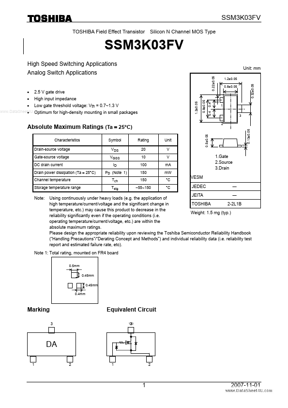
SSM3K03FV Overview
Key Features
- 2.5 V gate drive
- Low gate threshold voltage: Vth = 0.7~1.3 V
| Part | SSM3K03FV |
|---|---|
| Description | High Speed Switching Applications |
| Manufacturer | Toshiba |
| Size | 558.18 KB |
| Seller | Inventory | Price Breaks | Buy |
|---|---|---|---|
| UnikeyIC | 400000 | 700+ : 0.0219 USD 1400+ : 0.0215 USD 2100+ : 0.0209 USD |
View Offer |
| Unikeyic (ICkey) | 400000 | 700+ : 0.0219 USD 1400+ : 0.0215 USD 2100+ : 0.0209 USD |
View Offer |
| Part Number | Manufacturer | Description |
|---|---|---|
| I.MX31 | Freescale Semiconductor | Multimedia Applications Processors |
| i.MX28 | NXP Semiconductors | Applications Processors |
| i.MX35 | Freescale Semiconductor | Applications Processors |