• Part: SSM3K04FV
  • Description: High Speed Switching Applications
  • Manufacturer: Toshiba
  • Size: 559.53 KB
Download SSM3K04FV Datasheet PDF
Toshiba
SSM3K04FV
SSM3K04FV is High Speed Switching Applications manufactured by Toshiba.
TOSHIBA Field Effect Transistor Silicon N Channel MOS Type High Speed Switching Applications 0.22±0.05 Unit: mm 1.2±0.05 0.8±0.05 0.32±0.05 3 2 0.13±0.05 - - - - 
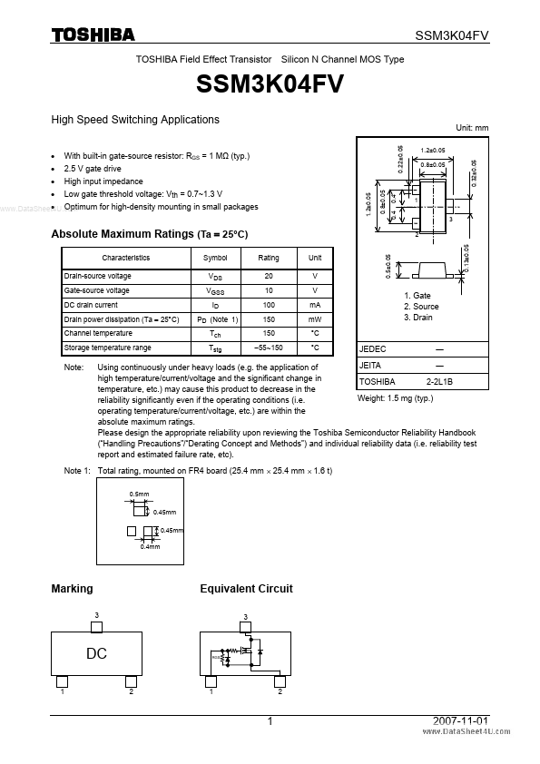
With built-in gate-source resistor: RGS = 1 MΩ (typ.) 2.5 V gate drive High input impedance 1.2±0.05 0.8±0.05 Low gate threshold voltage: Vth = 0.7~1.3 V Absolute Maximum Ratings (Ta = 25°C) Characteristics Drain-source voltage Gate-source voltage DC drain current Drain power dissipation (Ta = 25°C) Channel temperature Storage temperature range Symbol VDS VGSS ID PD (Note 1) Tch Tstg Rating 20 10 100 150 150 - 55~150 Unit V V m A m W °C °C 0.5±0.05 - Optimum for high-density mounting in small packages .. 1. Gate 2. Source 3. Drain JEDEC ― Note: JEITA ― Using continuously under heavy loads (e.g. the application of high temperature/current/voltage and the significant change in TOSHIBA 2-2L1B temperature, etc.) may cause this product to decrease in the Weight: 1.5 mg (typ.) reliability significantly even if the operating conditions (i.e. operating temperature/current/voltage, etc.) are within the absolute maximum ratings. Please design the appropriate reliability upon reviewing the Toshiba Semiconductor Reliability Handbook (“Handling Precautions”/“Derating Concept and Methods”) and individual reliability data (i.e. reliability test report and estimated failure rate, etc). Note 1: Total rating, mounted on FR4 board (25.4 mm × 25.4 mm × 1.6 t) 0.5mm 0.45mm 0.45mm 0.4mm Marking Equivalent Circuit 1 2 2007-11-01 Electrical Characteristics (Ta = 25°C) Characteristics Gate leakage current Drain-source breakdown voltage Drain cut-off current Gate threshold voltage Forward transfer admittance Drain-source on-resistance Input capacitance Reverse transfer capacitance .. Output capacitance Switching time Turn-on time Turn-off time Symbol IGSS V (BR) DSS IDSS Vth ⎪Yfs⎪ RDS (ON) Ciss Crss Coss ton toff RGS Test Condition VGS = 10 V, VDS = 0 ID...