SSM3K15ACT
TOSHIBA Field Effect Transistor Silicon N Channel MOS Type (U-MOS III)
Load Switching Applications
- 2.5 V drive
- Low ON-resistance: RDS(ON) = 3.6 Ω (max) (@VGS = 4 V)
RDS(ON) = 6.0 Ω (max) (@VGS = 2.5 V)
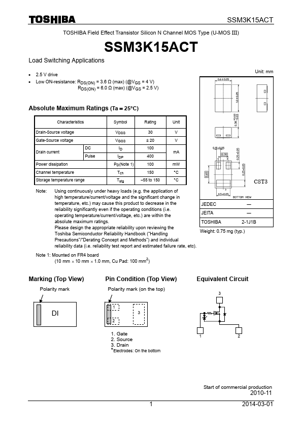
Unit: mm
Absolute Maximum Ratings (Ta = 25°C)
Characteristics
Symbol
Rating
Unit
Drain-Source voltage
Gate-Source voltage
Drain current
DC Pulse
Power dissipation
Channel temperature
Storage temperature range
VDSS
VGSS
± 20
100 m A
PD(Note 1)
100 m W
Tch
°C
Tstg
- 55 to 150
°C
CST3
Note:
Using continuously under heavy loads (e.g. the application of high temperature/current/voltage and the significant change in temperature, etc.) may cause this product to decrease in the
JEDEC
― reliability significantly even if the operating conditions (i.e. operating temperature/current/voltage, etc.) are within...