SSM3K16FS
TOSHIBA Field Effect Transistor Silicon N Channel MOS Type
High Speed Switching Applications Analog Switch Applications
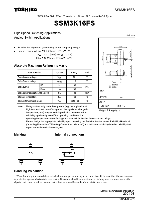
Unit: mm
- Suitable for high-density mounting due to pact package
- Low on resistance: Ron = 3.0 Ω (max) (@VGS = 4 V)
: Ron = 4.0 Ω (max) (@VGS = 2.5 V) : Ron = 15 Ω (max) (@VGS = 1.5 V)
Absolute Maximum Ratings (Ta = 25°C)
Characteristics
Symbol
Rating
Unit
Drain-Source voltage
Gate-Source voltage
VGSS
±10
Drain current
DC Pulse
100 m A
Drain power dissipation (Ta = 25°C)
100 m W
Channel temperature
Tch
°C
JEDEC
―
Storage temperature range
Tstg
- 55 to 150
°C
JEITA
―
Note:
Using continuously under heavy loads (e.g. the application...