SSM6N15AFU
Description
SSM6N15AFU TOSHIBA Field Effect Transistor Silicon N Channel MOS Type (U-MOS III) SSM6N15AFU Load Switching Applications • • • 2.5 V drive N-ch 2-in-1 Low ON-resistance: RDS(ON) = 3.6 Ω (max) (@VGS =...
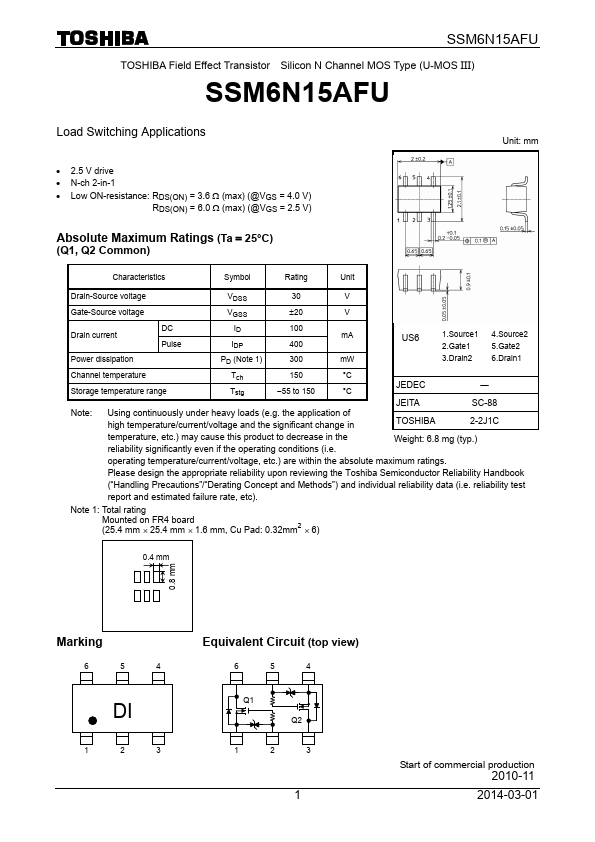
SSM6N15AFU TOSHIBA Field Effect Transistor Silicon N Channel MOS Type (U-MOS III) SSM6N15AFU Load Switching Applications • • • 2.5 V drive N-ch 2-in-1 Low ON-resistance: RDS(ON) = 3.6 Ω (max) (@VGS =...