The following content is an automatically extracted verbatim text
from the original manufacturer datasheet and is provided for reference purposes only.
View original datasheet text
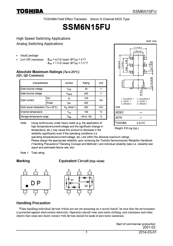
SSM6N15FU
TOSHIBA Field Effect Transistor Silicon N Channel MOS Type
SSM6N15FU
High Speed Switching Applications Analog Switching Applications
Unit: mm
• Small package
• Low ON resistance : Ron = 4.0 Ω (max) (@VGS = 4 V) : Ron = 7.0 Ω (max) (@VGS = 2.5 V)
Absolute Maximum Ratings (Ta = 25°C)
(Q1, Q2 Common)
Characteristics
Symbol
Rating
Unit
Drain-Source voltage
VDS
30
V
Gate-Source voltage
VGSS
±20
V
Drain current
DC Pulse
ID
100
mA
IDP
200
Drain power dissipation (Ta = 25°C)
PD (Note 1)
200
mW
Channel temperature
Tch
150
°C
JEDEC
―
Storage temperature range
Tstg
−55 to 150
°C
JEITA
―
Note:
Using continuously under heavy loads (e.g. the application of
TOSHIBA
2-2J1C
high temperature/current/voltage and the significant change in temperature, etc.