SSM6N16FU
Description
SSM6N16FU TOSHIBA Field Effect Transistor Silicon N Channel MOS Type SSM6N16FU High Speed Switching Applications Analog Switch Applications Unit: mm • Suitable for high-density mounting due to comp...
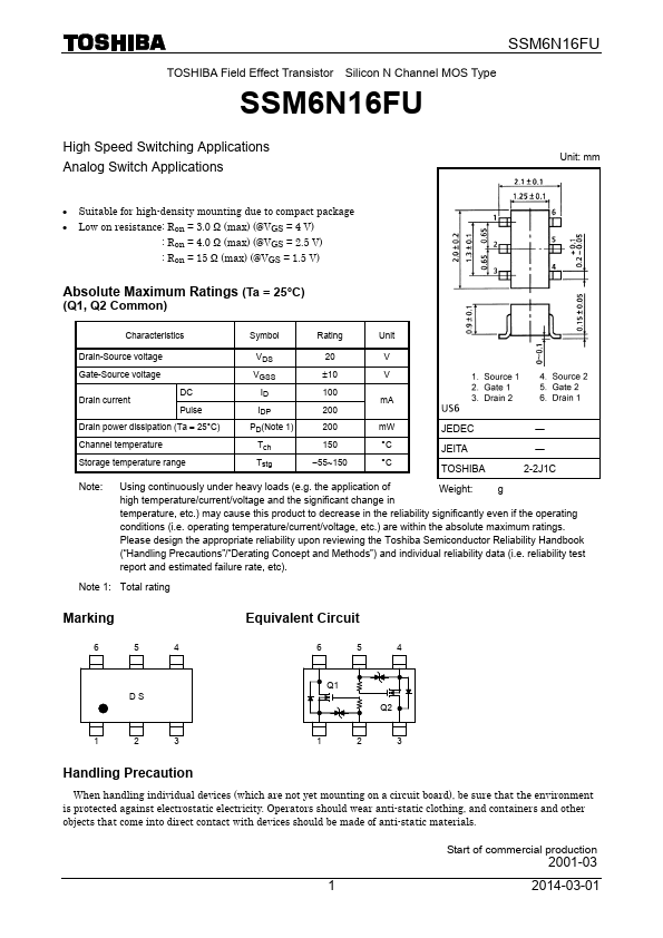
SSM6N16FU TOSHIBA Field Effect Transistor Silicon N Channel MOS Type SSM6N16FU High Speed Switching Applications Analog Switch Applications Unit: mm • Suitable for high-density mounting due to comp...