SSM3K15ACTC
Features
(1) 2.5 V drive (2) Low drain-source on-resistance
: RDS(ON) = 3.6 Ω (max) (@VGS = 4 V) RDS(ON) = 6.0 Ω (max) (@VGS = 2.5 V)
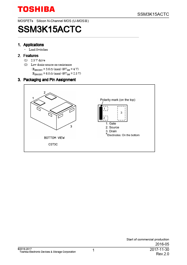
3. Packaging and Pin Assignment
CST3C
©2016-2017 Toshiba Electronic Devices & Storage Corporation
Start of mercial production
2016-05
2017-11-30 Rev.2.0
4. Absolute Maximum Ratings (Note) (Unless otherwise specified, Ta = 25 )
Characteristics
Symbol
Rating
Unit
Drain-source voltage
VDSS
Gate-source voltage
VGSS
±20
Drain current (DC)
(Note 1)
100 m A
Drain current (pulsed)
(Note 1)
Power dissipation
(Note 2)
500 m W
Channel temperature
Tch
Storage temperature
Tstg
-55 to...