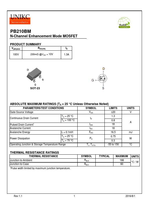
PB210BM Overview
| Part | PB210BM |
|---|---|
| Description | N-Channel MOSFET |
| Category | MOSFET |
| Manufacturer | UNIKC |
| Size | 876.82 KB |
| Seller | Inventory | Price Breaks | Buy |
|---|---|---|---|
| No distributor offers were returned for this part. | |||
| Part Number | Manufacturer | Description |
|---|---|---|
| PB210BD | VBsemi | N-Channel 100V MOSFET |
| PB210BD | NIKO-SEM | N-Channel MOSFET |
| PB2141 | Clear Microwave | Phase Shifter |
| PB2162A | HOTCHIP | mobile power SOC |