CHA5010B
CHA5010B is X Band Driver Amplifier manufactured by United Monolithic Semiconductors.
X Band Driver Amplifier
GaAs Monolithic Microwave IC
Description
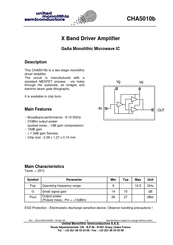
This CHA5010b is a two-stage monolithic driver amplifier. The circuit is manufactured with a standard MESFET process : via holes through the substrate, air bridges and electron beam gate lithography.
It is available in chip form.
Vg
Main Features
¦ Broadband performance : 9-10.5GHz ¦ 27dBm output power
(pulsed meas., -1dB gain pression) ¦ 15dB gain ¦ ± 1.5dB gain flatness ¦ Chip size : 2,09 x 1,27 x 0.10 mm
Vd OUT
Main Characteristics
Tamb. = 25°C
Symbol
Parameter
Fop Operating frequency range
G Pout
Small signal gain
Output power (Pulsed meas., Pin = +13dBm)
Min Typ Max Unit
9 10.5 GHz
14 15...