SiHF9Z24L
SiHF9Z24L is Power MOSFET manufactured by Vishay.
FEATURES
- Halogen-free According to IEC 61249-2-21
Definition
- Advanced Process Technology
- Surface Mount (IRF9Z24S, Si HF9Z24S)
- Low-Profile Through-Hole (IRF9Z24L, Si HF9Z24L)
- 175 °C Operating Temperature
- Fast Switching
- P-Channel
- Fully Avalanche Rated
- pliant to Ro HS Directive 2002/95/EC
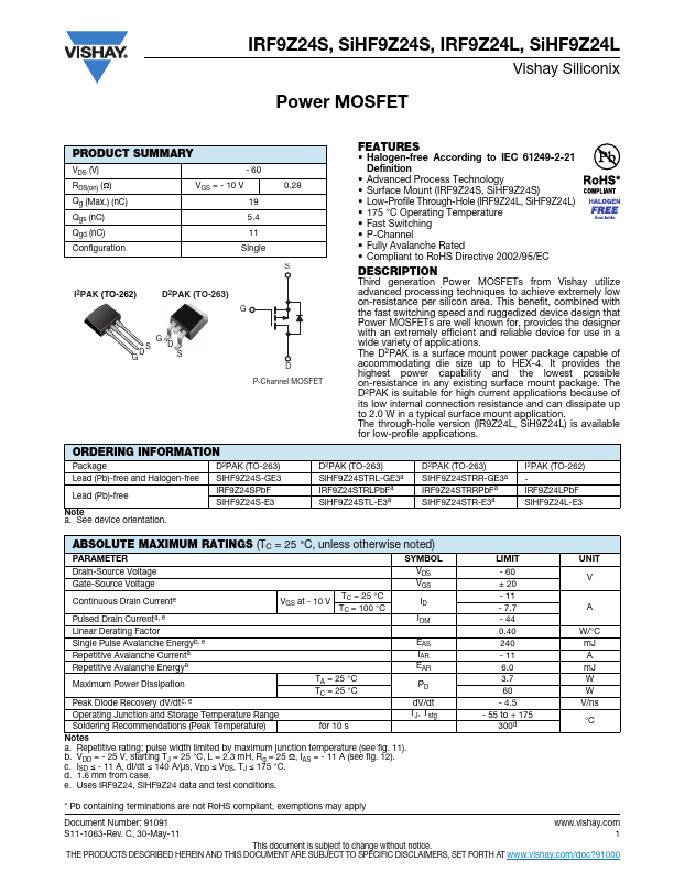
DESCRIPTION
Third generation Power MOSFETs from Vishay utilize advanced processing techniques to achieve extremely low on-resistance per silicon area. This benefit, bined with the fast switching speed and ruggedized device design that Power MOSFETs are well known for, provides the designer with an extremely efficient and reliable device for use in a wide variety of applications. The D2PAK is a surface mount power package capable of acmodating die size up to HEX-4. It provides the highest power capability and the lowest possible on-resistance in any existing surface mount package. The D2PAK is suitable for high current applications because of its low internal connection resistance and can dissipate up to 2.0 W in a typical surface mount application. The through-hole version (IR9Z24L, Si H9Z24L) is available for low-profile applications.
ORDERING INFORMATION
Package
D2PAK (TO-263)
Lead (Pb)-free and Halogen-free Si HF9Z24S-GE3
Lead (Pb)-free Note a. See device orientation.
IRF9Z24SPb F Si HF9Z24S-E3
D2PAK (TO-263) Si HF9Z24STRL-GE3a IRF9Z24STRLPb Fa Si HF9Z24STL-E3a
D2PAK (TO-263) Si HF9Z24STRR-GE3a IRF9Z24STRRPb Fa Si HF9Z24STR-E3a
I2PAK (TO-262) IRF9Z24LPb F Si HF9Z24L-E3
ABSOLUTE MAXIMUM RATINGS (TC = 25 °C, unless otherwise noted)
PARAMETER
SYMBOL
Drain-Source Voltage Gate-Source Voltage
VDS VGS
Continuous Drain Currente Pulsed Drain Currenta, e
VGS at
- 10 V
TC = 25 °C TC = 100 °C
ID IDM
Linear Derating Factor
Single Pulse Avalanche Energyb, e Repetitive Avalanche Currenta Repetitive Avalanche Energya
EAS IAR EAR
Maximum Power Dissipation
Peak Diode Recovery d V/dtc, e Operating Junction and Storage Temperature Range
TA = 25 °C TC = 25 °C
PD d V/dt TJ,...