WCSS0418V1P
Features
- Supports 100-MHz bus for Pentium and Power PC™ operations with zero wait states
- Fully registered inputs and outputs for pipelined operation
- 256K by 18 mon I/O architecture
- 3.3V core power supply
- 2.5V / 3.3V I/O operation
- Fast clock-to-output times ..
- 3.5 ns (for 166-MHz device)
- 4.0 ns (for 133-MHz device)
- -
- -
- -
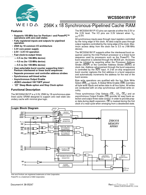
- 5.5 ns (for 100-MHz device) User-selectable burst counter supporting Intel Pentium interleaved or linear burst sequences Separate processor and controller address strobes Synchronous self-timed writes Asynchronous Output Enable JEDEC-standard 100 TQFP pinout “ZZ” Sleep Mode option and Stop Clock option The WCSS0418V1P I/O pins can operate at either the 2.5V or the 3.3V level. The I/O pins are 3.3V tolerant when VDDQ=2.5V. All synchronous inputs pass through input registers controlled by the rising edge of the clock. All data outputs pass through output registers controlled by the rising edge of the clock. Maximum access delay from the clock...