WT-2300
WT-2300 is Surface Mount N-Channel Enhancement Mode MOSFET manufactured by Weitron Technology.
Features
:
- Super high dense cell design for low RDS(ON) R DS(ON) <40 mΩ @VGS =4.5V R DS(ON) <60 mΩ @VGS =2.5V R DS(ON) <75 mΩ @VGS =1.8V
- Rugged and Reliable
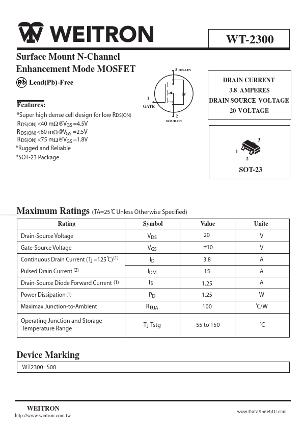
- SOT-23 Package
DRAIN SOURCE VOLTAGE 20 VOLTAGE
SOURCE
GATE
3 1 2
SOT-23
..
Maximum Ratings (TA=25 C Unless Otherwise Specified)
Rating Drain-Source Voltage Gate-Source Voltage Continuous Drain Current (TJ =125 C) (1) Pulsed Drain Current (2) Drain-Source Diode Forward Current (1) Power Dissipation (1) Maximax Junction-to-Ambient Operating Junction and Storage Temperature Range Symbol VDS VGS ID IDM IS PD R θ JA TJ, Tstg Value 20 Unite V V A A A W C/W C
+10 3.8 15 1.25 1.25 100 -55 to 150
Device Marking
WT2300=S00
WEITRON http://.weitron..tw
Electrical Characteristics
Characteristic (TA=25 C Unless otherwise noted) Symbol
V(BR)DSS VGS (th) IGSS IDSS
Min
Typ
Max
Unit
Static (2)
Drain-Source Breakdown Voltage VGS=0V, ID=250 u A Gate-Source Threshold Voltage VDS=VGS, ID=250 u A Gate-Source Leakage Current +10V VDS=0V, VGS=Zero Gate Voltage Drain Current VDS=20V, VGS=0V Drain-Source On-Resistance VGS=4.5V, ID=5.0A VGS=2.5V, ID=4.0A VGS=1.8V, ID=1.0A On-State Drain Current VDS=5V, VGS=4.5A Forward Transconductance VDS=5V, ID=5A 20 0.6 0.78 1.5 +100 1 40 60 75 V V n A u A mΩ
18 5 r DS (on)
32 50 62
ID(on) gfs
- -
Dynamic (3)
Input Capacitance VDS=15V, VGS=0V, f=1MHZ Output Capacitance VDS=15V, VGS=0V, f=1MHZ Reverse Transfer Capacitance VDS=15V, VGS=0V, f=1MHZ Ciss Coss Crss
- 888 144 115
Switching (3)
Turn-On Delay Time VGS =4.5V,V DD=10V, I D=1A, R L =10 Ω ,R GEN=6Ω Rise Time VGS =4.5V,V DD=10V, I D=1A, R L =10 Ω ,R GEN=6Ω Turn-Off Delay Time VGS =4.5V,V DD=10V, I D=1A, R L =10 Ω ,R GEN=6Ω Fall Time VGS =4.5V,V DD=10V, I D=1A, R L =10 Ω ,R GEN=6Ω Total Gate Charge VDS=10V, ID=3.5A, VGS =4.5V Gate-Source Charge VDS=10V, ID=3.5A, VGS =4.5V Gate-Drain Charge VDS=10V, ID=3.5A, VGS =4.5V Drain-Source Diode Forward Voltage VGS=0V, IS=1.25A td(on) tr td(off ) tf Qg Qgs Qgd
- 31.8...