W3E16M64S-XBX
W3E16M64S-XBX is 16Mx64 DDR SDRAM manufactured by White Electronic.
FEATURES
DDR Data Rate = 200, 250, 266Mbps Package:
- 219 Plastic Ball Grid Array (PBGA), 21 x 25mm 2.5V ±0.2V core power supply 2.5V I/O (SSTL_2 patible) Differential clock inputs (CLK and CLK#) mands entered on each positive CLK edge Internal pipelined double-data-rate (DDR) architecture; two data accesses per clock cycle Programmable Burst length: 2,4 or 8 Bidirectional data strobe (DQS) transmitted/ received with data, i.e., source-synchronous data capture (one per byte) DQS edge-aligned with data for READs; centeraligned with data for WRITEs DLL to align DQ and DQS transitions with CLK
..
BENEFITS
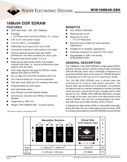
50% SPACE SAVINGS Reduced part count Reduced I/O count
- 17% I/O Reduction Reduced trace lengths for lower parasitic capacitance Suitable for hi-reliability applications Laminate interposer for optimum TCE match Upgradeable to 32M x 64 density (W3E32M64S-XBX)
GENERAL DESCRIPTION
The 128MByte (1Gb) DDR SDRAM is a high-speed CMOS, dynamic random-access, memory using 4 chips containing 268,435,456 bits. Each chip is internally configured as a quad-bank DRAM. Each of the chip’s 67,108,864-bit banks is organized as 8,192 rows by 512 columns by 16 bits. The 128 MB DDR SDRAM uses a double data rate architecture to achieve high-speed operation. The double data rate architecture is essentially a 2n-prefetch architecture with an interface designed to transfer two data words per clock cycle at the I/O pins. A single read or write access for the 128MB DDR SDRAM effectively consists of a single 2n-bit wide, one-clock-cycle data tansfer at the internal DRAM core and two corresponding n-bit wide, one-half-clock-cycle data transfers at the I/O pins. A bidirectional data strobe (DQS) is transmitted externally, along with data, for use in data capture at the receiver. DQS is a strobe transmitted by the DDR SDRAM during READs
Four internal banks for concurrent operation
Two data mask (DM) pins for masking write data Programmable IOL/IOH option Auto precharge option...