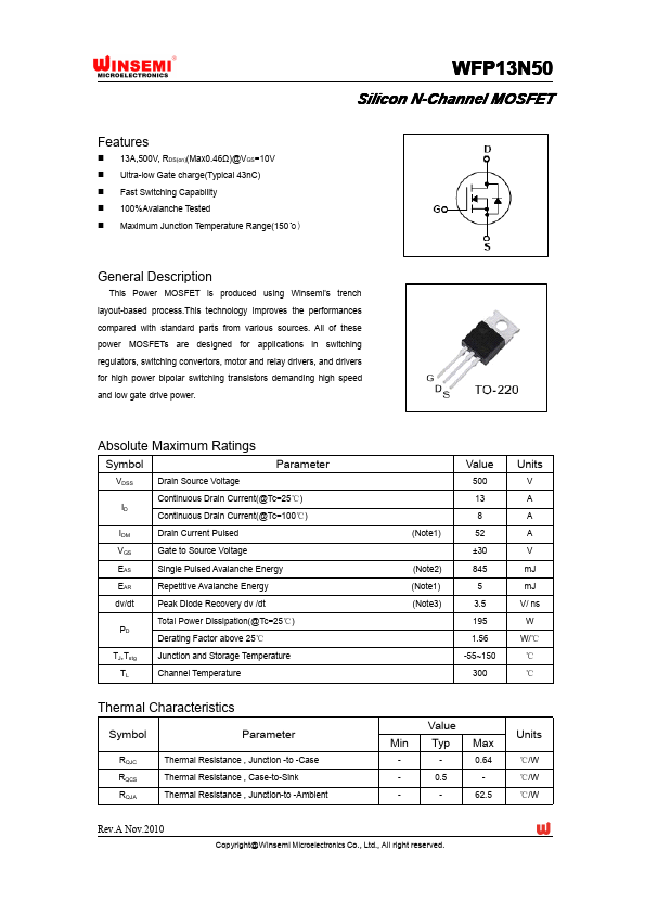
FEATURES
13A,500V, RDS(on)(Max0.46Ω)@VGS=10V Ultra-low Gate charge(Typical 43nC) Fast Switching Capability 100%Avalanche Tested Maximum Junction Temperature Range(150℃) WFP13N50 Silicon N-Channel MOSFET GENERAL DESCRIPTION
All of these power MOSFETs are designed for applications in switching regulators, switching convertors, motor and relay drivers, and drivers for high power bipolar switching transistors demanding high speed and low gate drive power. ABSOLUTE MAXIMUM RATINGS
Symbol Parameter VDSS ID Drain Source Voltage Continuous Drain Current(@Tc=25℃) Continuous Drain Current(@Tc=100℃) IDM Drain Current Pulsed VGS Gate to Source Voltage EAS Single Pulsed Avalanche Energy EAR Repetitive Avalanche Energy dv/dt Peak Diode Recovery dv /dt Total Power Dissipation(@Tc=25℃) PD Der Winsemi