CDC329A
CDC329A is 1-Line To 6-Line Clock Driver manufactured by Texas Instruments.
- Part of the CDC398A comparator family.
- Part of the CDC398A comparator family.
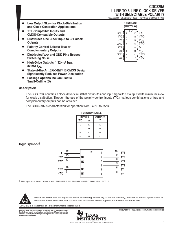
description
The CDC329A contains a clock-driver circuit that distributes one input signal to six outputs with minimum skew for clock distribution. Through the use of the polarity-control inputs (T/C), various binations of true and plementary outputs can be obtained.
The CDC329A is characterized for operation from
- 40°C to 85°C.
FUNCTION TABLE
INPUTS T/C A
OUTPUT Y
L logic symbol†
1T/C
N1
2T/C
N2
3T/C
N3
4T/C
N4
1Y1
1Y2
2Y1...