CDCLVP2104 Description
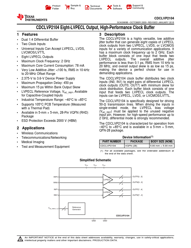
The CDCLVP2104 is a highly versatile, low additive jitter buffer that can generate eight copies of LVPECL clock outputs from two LVPECL, LVDS, or LVCMOS inputs for a variety of munication applications. It has a maximum clock frequency up to 2 GHz. Each buffer block consists of one input that feeds two LVPECL outputs.
CDCLVP2104 Key Features
- 1 Dual 1:4 Differential Buffer
- Two Clock Inputs
- Universal Inputs Can Accept LVPECL, LVDS
- Eight LVPECL Outputs
- Maximum Clock Frequency: 2 GHz
- Maximum Core Current Consumption: 78 mA
- Very Low Additive Jitter: <100 fs, RMS in 10-kHz
- 2.375-V to 3.6-V Device Power Supply
- Maximum Propagation Delay: 450 ps
- Maximum 15 ps Within Bank Output Skew