CDCVF2510A Description
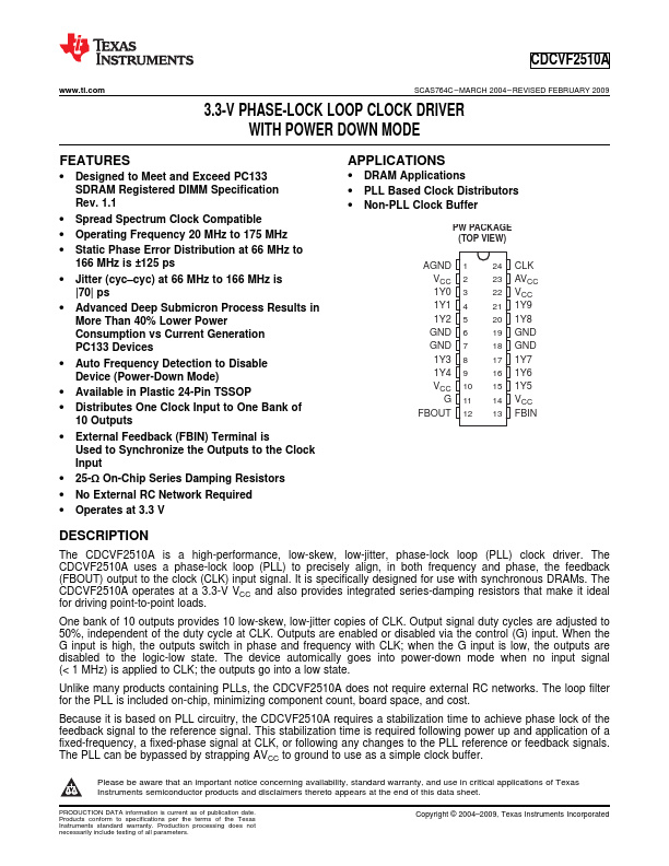
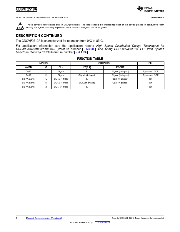
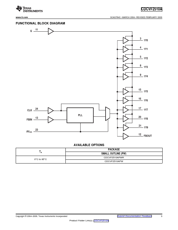
The CDCVF2510A is a high-performance, low-skew, low-jitter, phase-lock loop (PLL) clock driver. The CDCVF2510A uses a phase-lock loop (PLL) to precisely align, in both frequency and phase, the feedback (FBOUT) output to the clock (CLK) input signal. It is specifically designed for use with synchronous DRAMs.
CDCVF2510A Key Features
- Designed to Meet and Exceed PC133 SDRAM Registered DIMM Specification Rev. 1.1
- Spread Spectrum Clock patible
- Operating Frequency 20 MHz to 175 MHz
- Jitter (cyc-cyc) at 66 MHz to 166 MHz is |70| ps
- Advanced Deep Submicron Process Results in More Than 40% Lower Power Consumption vs Current Generation PC133 Devices
- Auto Frequency Detection to Disable Device (Power-Down Mode)
- Available in Plastic 24-Pin TSSOP
- External Feedback (FBIN) Terminal is Used to Synchronize the Outputs to the Clock Input
- 25-Ω On-Chip Series Damping Resistors
- No External RC Network Required