LMK00334 Overview
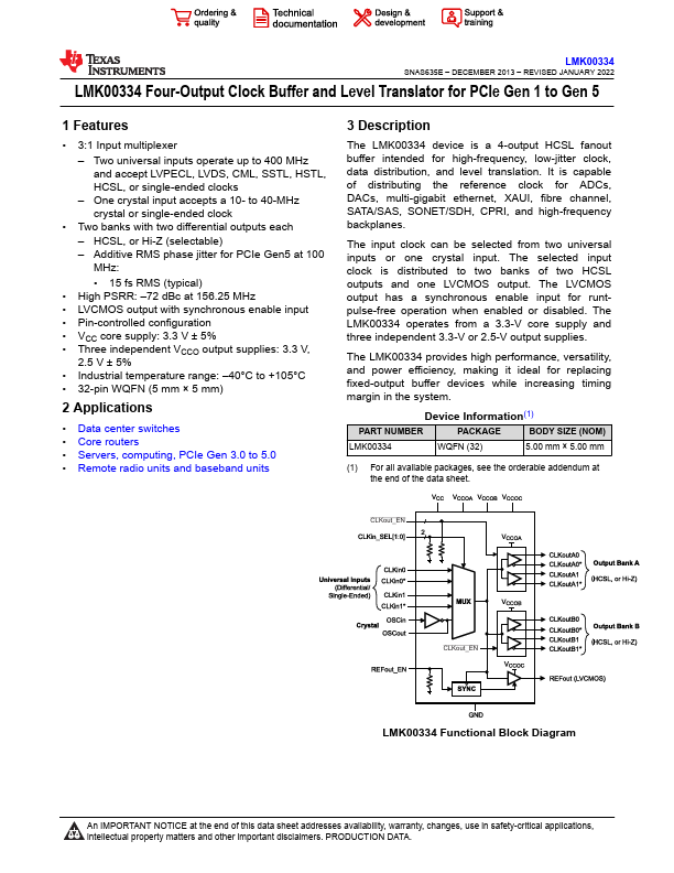
The LMK00334 device is a 4-output HCSL fanout buffer intended for high-frequency, low-jitter clock, data distribution, and level translation. It is capable of distributing the reference clock for ADCs, DACs, multi-gigabit ethernet, XAUI, fibre channel, SATA/SAS, SONET/SDH, CPRI, and high-frequency backplanes. The input clock can be selected from two universal inputs or one crystal input.
LMK00334 Key Features
- 3:1 Input multiplexer
- Two universal inputs operate up to 400 MHz and accept LVPECL, LVDS, CML, SSTL, HSTL, HCSL, or single-ended clocks
- One crystal input accepts a 10- to 40-MHz crystal or single-ended clock
- Two banks with two differential outputs each
- HCSL, or Hi-Z (selectable)
- Additive RMS phase jitter for PCIe Gen5 at 100
- 15 fs RMS (typical)
- High PSRR: -72 dBc at 156.25 MHz
- LVCMOS output with synchronous enable input
- Pin-controlled configuration