LMK00338 Description
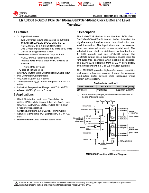
The LMK00338 device is an 8-output PCIe Gen1/ Gen2/Gen3/Gen4/Gen5 fanout buffer intended for high-frequency, low-jitter clock, data distribution, and level translation. The input clock can be selected from two universal inputs or one crystal input. The selected input clock is distributed to two banks of 4 HCSL outputs and one LVCMOS output.
LMK00338 Key Features
- 3:1 Input Multiplexer
- Two Universal Inputs Operate up to 400 MHz and Accept LVPECL, LVDS, CML, SSTL, HSTL, HCSL, or Single-Ended Clocks
- One Crystal Input Accepts a 10-MHz to 40-MHz Crystal or Single-Ended Clock
- Two Banks With 4 Differential Outputs Each
- HCSL, or Hi-Z (Selectable per Bank)
- Additive RMS Phase Jitter for PCIe Gen5 at
- 15 fs RMS (Typical)
- 72 dBc at 156.25 MHz
- LVCMOS Output With Synchronous Enable Input
- Pin-Controlled Configuration
LMK00338 Applications
- Clock Distribution and Level Translation for ADCs, DACs, Multi-Gigabit Ethernet, XAUI, Fibre Channel, SATA/SAS, SONET/SDH, CPRI, HighFrequency Backplanes