TMS320TCI6488 Description
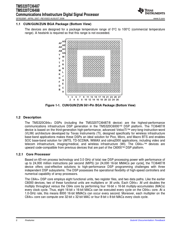
TMS320TCI6487 TMS320TCI6488 munications Infrastructure Digital Signal Processor SPRS358F APRIL 2007 REVISED AUGUST 2008.
TMS320TCI6488 Key Features
- High-Performance munications Infrastructure DSP (TCI6487/8)
- 1-ns Instruction Cycle Time
- 1.0-GHz Clock Rate
- Eight 32-Bit Instructions/Cycle
- mercial Temperature 0°C to 100°C
- 3 TMS320C64x+™ DSP Cores
- Dedicated SPLOOP Instructions
- pact Instructions (16-Bit)
- Exception Handling
- TMS320C64x+ Megamodule L1/L2 Memory Architecture