74VHCT595 Description
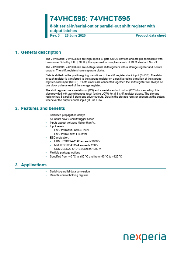
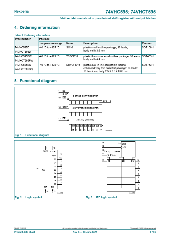
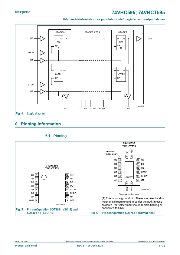
74VHCT595 are high-speed Si-gate CMOS devices and are pin patible with Low-power Schottky TTL (LSTTL). It is specified in pliance with JEDEC standard No. 74VHCT595 are 8-stage serial shift registers with a storage register and 3-state outputs.
74VHCT595 Key Features
- Balanced propagation delays
- All inputs have Schmitt-trigger action
- Inputs accept voltages higher than VCC
- Input levels
- For 74VHC595: CMOS level
- For 74VHCT595: TTL level
- ESD protection
- HBM JESD22-A114F exceeds 2000 V
- MM JESD22-A115-A exceeds 200 V
- CDM JESD22-C101E exceeds 1000 V
74VHCT595 Applications
- Serial-to-parallel data conversion