PED2312
PED2312 is Dual P & N-Channel Enhancement Mode Power MOSFET manufactured by semi one.
DESCRIPTION
The PED2312 uses advanced trench technology to provide excellent RDS(ON), low gate charge and operation with gate voltages as low as 2.5V. This device is suitable for use as a load switch or in PWM applications.
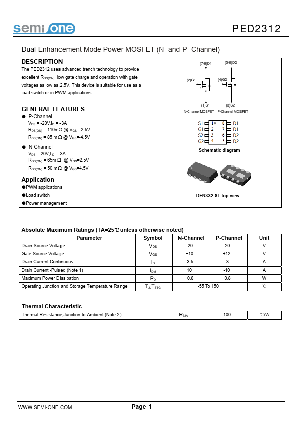
(7/8)D1
(5/6)D2
(2)G1
(4)G2
GENERAL FEATURES
- P-Channel VDS = -20V,ID = -3A RDS(ON) = 110mΩ @ VGS=-2.5V RDS(ON) = 85 m Ω @ VGS=-4.5V
- N-Channel VDS = 20V,I D = 3A RDS(ON) = 65m Ω @ VGS=2.5V RDS(ON) = 50 m Ω @ VGS=4.5V
Application
- PWM applications
- Load switch
- Power management
(1)S1
(3)S2
N-Channel MOSFET P-Channel MOSFET
Schematic diagram
DFN3X2-8L top view
Absolute Maximum Ratings (TA=25℃unless otherwise noted)
Parameter
Symbol
N-Channel P-Channel
Drain-Source Voltage
VDS 20 -20
Gate-Source Voltage
±10
±12
Drain Current-Continuous
ID 3.5 -3
Drain Current -Pulsed (Note 1) Maximum Power Dissipation Operating Junction and Storage Temperature...