PED3312M
PED3312M is N-Channel Enhancement Mode Power MOSFET manufactured by semi one.
Description
The PED3312M uses advanced trench technology to provide excellent RDS(ON) and low gate charge. It can be used in a wide variety of applications. It is ESD protected.
General Features
- VDS = 18V, ID = 22 A
RDS(ON) < 4.3mΩ @ VGS=4.5V RDS(ON) < 4.6mΩ @ VGS=3.8V RDS(ON) < 5.0mΩ @ VGS=3.0V RDS(ON) < 6.8mΩ @ VGS=2.5V ESD Rating: 4000V HBM
- High Power and current handing capability
- Lead free product is acquired
- Surface Mount Package
Application
- PWM applications
- Load switch
- Power management
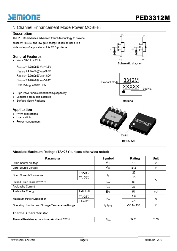
Schematic diagram Marking
DFN3x3-8L
Absolute Maximum Ratings (TA=25℃ unless otherwise noted)
Drain-Source Voltage Gate-Source Voltage
Parameter
Drain Current-Continuous
Pulsed Drain Current (Note 1) Avalanche Current Avalanche Energy
Maximum Power Dissipation Operating Junction and Storage Temperature Range
TA=25℃ TA=70℃
L=0.1m H TA=25℃ TA=70℃
Symbol
VDS VGS
IDM IAS EAS
PD TJ,TSTG
Thermal Characteristic
Thermal Resistance, Junction-to-Ambient (Note 2)
RθJA
Rating
18 ±12 22 16 80 33 54 3.6 2.4 -55 To 150
Unit
A m J W ℃
℃/W
.semi-one.
Page 1
2020 Jun....