2SK2112 Datasheet
2SK2112 Datasheet (Renesas)
Renesas
DATA SHEET MOS FIELD EFFECT TRANSISTOR 2SK2112 N-CHANNEL MOS FET FOR HIGH-SPEED SWITCHING The 2SK2112 is a N-channel MOS FET of a vertical type and is a switching element that can be directly driven .
* Low ON resistance
RDS(on) = 1.2 Ω MAX. @VGS = 4.0 V, ID = 0.5 A
* High switching speed
ton + toff < 100 ns
* Low parasitic capacitance
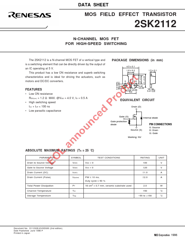
PACKAGE DIMENSIONS (in mm)
4.5 ± 0.1 1.6 ± 0.2
1.5 ± 0.1
0.8 MIN. 2.5 ± 0.1
4.0 ± 0.25
SDG
0.42 ±0.06 1.5
0.42 0.47 ±0.06 ±0.06
3.0
0.41+
*00..0053
EQUIVA.
2SK2112 Datasheet (VBsemi)
VBsemi
2SK2112-VB 2SK2112-VB Datasheet N-Channel 100 V (D-S) MOSFET MOSFET PRODUCT SUMMARY VDS (V) RDS(on) () Typ. ID (A)a 0.102 at VGS = 10 V 4.2 100 0.120 at VGS = 6 V 3.8 0.125.
* Trench Power MOSFET
* 100 % Rg and UIS Tested
APPLICATIONS
* DC/DC Converters / Boost Converters
* Load Switch
* LED Backlighting in LCD TVs
* Power Management for Mobile Computing
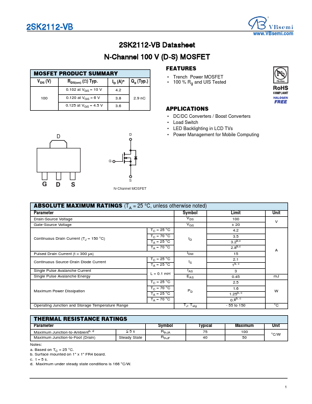
G
GD S
S N-Channel MOSFET
ABSOLUTE MAXIMUM RATINGS (TA = 25 °C, unless otherwise noted)
Parameter
Symbol
Drain.
2SK2112 Datasheet (Kexin Semiconductor)
Kexin Semiconductor
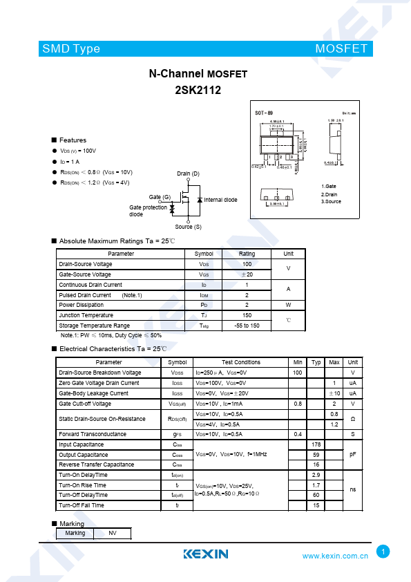
SMD Type N-Channel MOSFET 2SK2112 MOSFET 1.70 0.1 ■ Features ● VDS (V) = 100V ● ID = 1 A ● RDS(ON) < 0.8Ω (VGS = 10V) ● RDS(ON) < 1.2Ω (VGS = 4V) Drain (D) Gate (G) Gate protection diode Intern.
* VDS (V) = 100V
* ID = 1 A
* RDS(ON) < 0.8Ω (VGS = 10V)
* RDS(ON) < 1.2Ω (VGS = 4V)
Drain (D)
Gate (G)
Gate protection diode
Internal diode
Source (S)
0.42 0.1
0.46 0.1
1.Gate 2.Drain 3.Source
* Absolute Maximum Ratings Ta = 25℃
Parameter Drain-Source Voltage Gate-Source Voltage Continuous.
2SK2112 Datasheet (NEC)
NEC
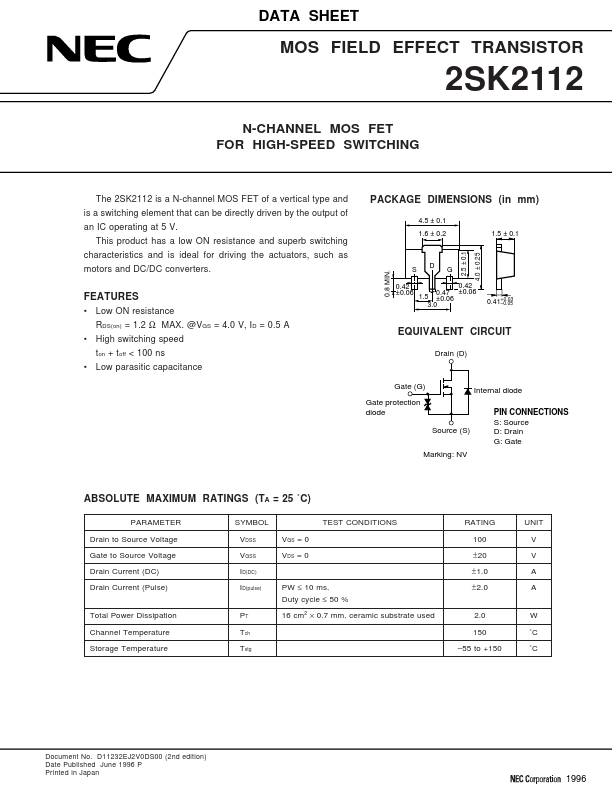
DATA SHEET MOS FIELD EFFECT TRANSISTOR 2SK2112 N-CHANNEL MOS FET FOR HIGH-SPEED SWITCHING The 2SK2112 is a N-channel MOS FET of a vertical type and is a switching element that can be directly drive.
* Low ON resistance RDS(on) = 1.2 Ω MAX. @VGS = 4.0 V, ID = 0.5 A
* High switching speed ton + toff < 100 ns
* Low parasitic capacitance
0.42 0.47 ±0.06 1.5 ±0.06 3.0
0.41+0.03
*0.05
EQUIVALENT CIRCUIT
Drain (D)
Gate (G) Gate protection diode Source (S) Marking: NV
Internal diode PIN CONNECTION.