2SK2112 Overview
Key Specifications
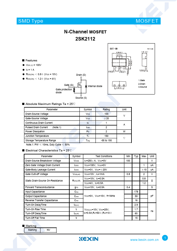
Package: SC
Mount Type: Surface Mount
Pins: 3
Height: 1.6 mm
Key Features
- VDS (V) = 100V
- RDS(ON) < 0.8Ω (VGS = 10V)
- RDS(ON) < 1.2Ω (VGS = 4V) Drain (D) Gate (G) Gate protection diode Internal diode Source (S) 0.42 0.1 0.46 0.1