Datasheet Details
| Part number | AOD482 |
|---|---|
| Manufacturer | Alpha & Omega Semiconductors |
| File Size | 394.58 KB |
| Description | 100V N-Channel MOSFET |
| Datasheet |
 AOD482 Datasheet AOD482 Datasheet
|
|
|
| Part number | AOD482 |
|---|---|
| Manufacturer | Alpha & Omega Semiconductors |
| File Size | 394.58 KB |
| Description | 100V N-Channel MOSFET |
| Datasheet |
AOD482 Datasheet
|
|
|
|
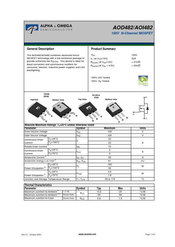
The AOD482/AOI482 combines advanced trench MOSFET technology with a low resistance package to provide extremely low RDS(ON).
This device is ideal for boost converters and synchronous rectifiers for consumer, telecom, industrial power supplies and LED backlighting.
Product Summary VDS ID (at VGS=10V) RDS(ON) (at VGS=10V) RDS(ON) (at VGS = 4.5V) 100% UIS Tested 100% Rg Tested 100V 32A < 37mW < 42mW TO252 DPAK TO-251A IPAK D TopView Bottom View Top View Bottom View D D DS G DG S S D G G G D S Absolute Maximum Ratings TA=25°C unless otherwise noted Parameter Symbol Maximum Drain-Source Voltage VDS 100 Gate-Source Voltage VGS ±20 Continuous Drain Current TC=25°C TC=100°C ID 32 22 Pulsed Drain Current C IDM 70 Continuous Drain Current TA=25°C TA=70°C IDSM 5 4 Avalanche Current C IAS, IAR 35 Avalanche energy L=0.1mH C EAS, EAR 61 TC=25°C Power Dissipation B TC=100°C PD 100 50 TA=25°C Power Dissipation A TA=70°C PDSM 2.5 1.6 Junction and Storage Temperature Range TJ, TSTG -55 to 175 Thermal Characteristics Parameter Maximum Junction-to-Ambient A Maximum Junction-to-Ambient A D Maximum Junction-to-Case t ≤ 10s Steady-State Steady-State Symbol RqJA RqJC Typ 14.2 39 0.8 Max 20 50 1.5 S Units V V A A A mJ W W °C Units °C/W °C/W °C/W Rev 2.1 : October 2023 www.aosmd.com Page 1 of 6 AOD482/AOI482 Electrical Characteristics (TJ=25°C unless otherwise noted) Symbol Parameter Conditions Min Typ Max Units STATIC PARAMETERS BVDSS Drain-Source Breakdown Voltage ID=250mA, VGS=0V 100 V IDSS Zero Gate Voltage Drain Current VDS=100V, VGS=0V TJ=55°C 1 mA 5 IGSS Gate-Body leakage current VDS=0V, VGS= ±20V 100 nA VGS(th) Gate Threshold Voltage VDS=VGS ID=250mA 1.6 2.1 2.7 V ID(ON) On state drain current VGS=10V, VDS=5V 70 A RDS(ON) Static Drain-Source On-Resistance VGS=10V, ID=10A TJ=125°C 30 37 mW 63 76 VGS=4.5V, ID=10A 32 42 mW gFS Fo
AOD482/AOI482 100V N-Channel MOSFET General.
| Brand Logo | Part Number | Description | Manufacturer |
|---|---|---|---|
| AOD482 | N-Channel MOSFET | INCHANGE |
| Part Number | Description |
|---|---|
| AOD480 | 30V N-Channel MOSFET |
| AOD484 | N-Channel MOSFET |
| AOD486A | 40V N-Channel MOSFET |
| AOD488 | N-Channel MOSFET |
| AOD400 | N-Channel MOSFET |
| AOD402 | N-Channel MOSFET |
| AOD403 | 30V P-Channel MOSFET |
| AOD404 | N-Channel MOSFET |
| AOD405 | P-Channel MOSFET |
| AOD406 | N-Channel Enhancement Mode Field Effect Transistor |