MX4953
Description
The MX4953 uses advanced trench technology to provide excellent RDS(ON), low gate charge and operation with gate voltages as low as -4.5V. This device is suitable for use as a load switch or in PWM applications.
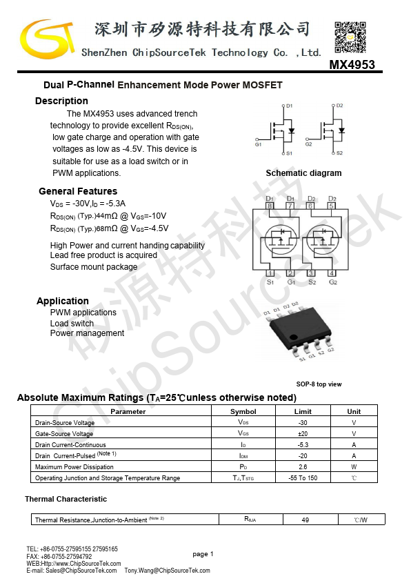
Schematic diagram
General Features
VDS = -30V,ID = -5.3A RDS(ON) (Typ.)44mΩ @ VGS=-10V
技 k RDS(ON) (Typ.)68mΩ @ VGS=-4.5V
High Power and current handing capability
科 e Lead free product is acquired T Surface mount package 特 e Application 源 rc PWM applications
Load switch u Power management
矽 So SOP-8 top view ip Absolute Maximum Ratings (TA=25℃unless otherwise noted) h Drain-Source Voltage
Parameter
Symbol VDS
Limit
Unit
-30
Gate-Source Voltage
±20
C Drain Current-Continuous
-5.3
Drain Current-Pulsed (Note 1)
-20
Maximum Power Dissipation
Operating Junction and Storage Temperature Range
TJ,TSTG
-55 To 150
℃
Thermal Characteristic
Thermal Resistance,Junction-to-Ambient (Note 2)
RθJA
℃/W
TEL:...