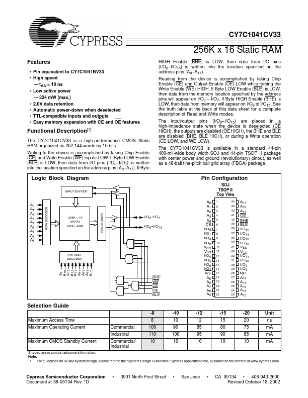
CY7C1041CV33 Overview
Key Features
- Pin equivalent to CY7C1041BV33
- Low active power
- 324 mW (max.)
- 2.0V data retention
- Automatic power-down when deselected
- TTL-compatible inputs and outputs
| Part | CY7C1041CV33 |
|---|---|
| Description | 256K x 16 Static RAM |
| Manufacturer | Cypress |
| Size | 226.39 KB |
| Part Number | Manufacturer | Description |
|---|---|---|
| HT16K33 | Holtek Semiconductor | RAM Mapping 16 x 8 LED Controller Driver |
| M58725P | Mitsubishi Electric | 16K-Bit Static RAM |
| HT1621B | HTCSEMI | RAM Mapping 32x4 LCD Controller |