CY7C1069DV33
Overview
- High speed ❐ tAA = 10 ns
- Low active power ❐ ICC = 175 mA at 100 MHz
- Low complementary metal oxide semiconductor (CMOS) standby power ❐ ISB2 = 25 mA
- Operating voltages of 3.3 ± 0.3 V
- 2.0 V data retention
- Automatic power-down when deselected
- Transistor-transistor logic (TTL) compatible inputs and outputs
- Easy memory expansion with CE1 and CE2 features
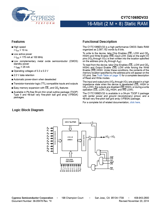
- Available in Pb-free 54-pin thin small outline package (TSOP) Type II and 48-ball very fine-pitch ball grid array (VFBGA) packages. Functional Description The CY7C1069DV33 is a high performance CMOS Static RAM organized as 2,097,152 words by 8 bits. To write to the device, take Chip Enables (CE1 LOW and CE2 HIGH) and Write Enable (WE) input LOW. Data on the eight I/O pins (I/O0 through I/O7) is then written into the location specified on the address pins (A0 through A20). To read from the device, take Chip Enables (CE1 LOW and CE2 HIGH) and Output Enable (OE) LOW while forcing the Write Enable (WE) HIGH. Under these conditions, the contents of the memory location specified by the address pins will appear on the I/O pins. See Truth Table on page 10 for a complete description of Read and Write modes. The input and output pins (I/O0 through I/O7) are placed in a high impedance state when the device is deselected (CE1 HIGH or CE2 LOW), the outputs are disabled (OE HIGH), or during a write operation (CE1 LOW, CE2 HIGH, and WE LOW). The CY7C1069DV33 is available in a 54-pin TSOP II package with center power and ground (revolutionary) pinout, and a 48-ball very fine-pitch ball grid array (VFBGA) package. For a complete list of related documentation, click here. Logic Block Diagram 13 14