Datasheet4U Logo Datasheet4U.com
Cypress (now Infineon) logo

CY7C1146V18 Datasheet

Manufacturer: Cypress (now Infineon)
CY7C1146V18 datasheet preview

Datasheet Details

Part number CY7C1146V18
Datasheet CY7C1146V18_CypressSemiconductor.pdf
File Size 1.15 MB
Manufacturer Cypress (now Infineon)
Description (CY7C11xxV18) 18-Mbit DDR-II SRAM 2-Word Burst Architecture
CY7C1146V18 page 2 CY7C1146V18 page 3

CY7C1146V18 Overview

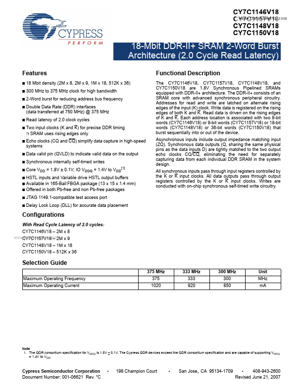
The DDR-II+ consists of an SRAM core with advanced synchronous peripheral circuitry. Addresses for read and write are latched on alternate rising edges of the input (K) clock. Write data is registered on the rising edges of both K.

CY7C1146V18 Key Features

  • Functional Description
  • SRAM uses rising edges only Echo clocks (CQ and CQ) simplify data capture in high-speed systems Data valid pin (QVLD) to
  • HSTL inputs and Variable drive HSTL output buffers
  • Available in 165-Ball FBGA package (13 x 15 x 1.4 mm)
  • Offered in both Pb-free and non Pb-free packages
  • 2M x 8
  • 2M x 9
  • 1M x 18 CY7C1150V18
  • 512K x 36
  • 198 Champion Court
Cypress (now Infineon) logo - Manufacturer

More Datasheets from Cypress (now Infineon)

See all Cypress (now Infineon) datasheets

Part Number Description
CY7C1141V18 (CY7C11xxV18) SRAM 4-Word Burst Architecture
CY7C1143KV18 18-Mbit QDR II+ SRAM Four-Word Burst Architecture
CY7C1143V18 (CY7C11xxV18) SRAM 4-Word Burst Architecture
CY7C1145KV18 18-Mbit QDR II+ SRAM Four-Word Burst Architecture
CY7C1145V18 (CY7C11xxV18) SRAM 4-Word Burst Architecture
CY7C1148KV18 18-Mbit DDR II+ SRAM Two-Word Burst Architecture
CY7C1148V18 (CY7C11xxV18) 18-Mbit DDR-II SRAM 2-Word Burst Architecture
CY7C1150KV18 18-Mbit DDR II+ SRAM Two-Word Burst Architecture
CY7C1150V18 (CY7C11xxV18) 18-Mbit DDR-II SRAM 2-Word Burst Architecture
CY7C1156V18 (CY7C11xxV18) SRAM 4-Word Burst Architecture

CY7C1146V18 Distributor

Datasheet4U Logo
Since 2006. D4U Semicon. About Datasheet4U Contact Us Privacy Policy Purchase of parts