Datasheet4U Logo Datasheet4U.com

CY7C1360V25 - 256K x 36/256K x 32/512K x 18 Pipelined SRAM

Description

The CY7C1360V25, CY7C1364V25 and CY7C1362V25 are 2.5V, 256K x 36, 256K x 32 and 512K x 18 synchronous-pipelined cache SRAM, respectively.

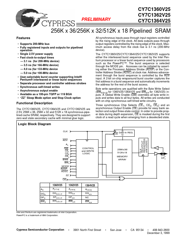
They are designed to support zero wait state secondary cache with minimal glue logic.

Features

  • Supports 200-MHz bus.
  • Fully registered inputs and outputs for pipelined operation.
  • Single 2.5V power supply.
  • Fast clock-to-output times.
  • 3.1 ns (for 200-MHz device).
  • 3.5 ns (for 166-MHz device).
  • 4.0 ns (for 133-MHz device.
  • 5.0 ns (for 100-MHz device.
  • User-selectable burst counter supporting Intel® Pentium® interleaved or linear burst sequences.
  • Separate processor and controller address strobes.
  • Sy.

📥 Download Datasheet

Other Datasheets by Cypress Semiconductor

Full PDF Text Transcription

Click to expand full text
PRELIMINARY CY7C1360V25 CY7C1362V25 CY7C1364V25 256K x 36/256K x 32/512K x 18 Pipelined SRAM Features • Supports 200-MHz bus • Fully registered inputs and outputs for pipelined operation • Single 2.5V power supply • Fast clock-to-output times — 3.1 ns (for 200-MHz device) — 3.5 ns (for 166-MHz device) — 4.0 ns (for 133-MHz device — 5.0 ns (for 100-MHz device • User-selectable burst counter supporting Intel® Pentium® interleaved or linear burst sequences • Separate processor and controller address strobes • Synchronous self-timed writes • Asynchronous output enable • Available as a 100-pin TQFP or 119 BGA • “ZZ” Sleep Mode option and Stop Clock option Functional Description The CY7C1360V25, CY7C1364V25 and CY7C1362V25 are 2.
Published: |