CY7C1371DV25 Overview
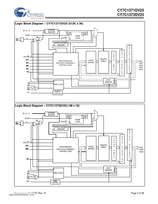
The CY7C1371DV25/CY7C1373DV25 is equipped with the advanced No Bus Latency (NoBL) logic required to enable consecutive Read/Write operations with data being transferred on every clock cycle.
CY7C1371DV25 Key Features
- No Bus Latency™ (NoBL™) architecture eliminates dead cycles between write and read cycles
- Can support up to 133-MHz bus operations with zero wait states
- Data is transferred on every clock
- Pin patible and functionally equivalent to ZBT™ devices
- Internally self-timed output buffer control to eliminate the need to use OE
- Registered inputs for flow-through operation
- Byte Write capability
- 2.5V core power supply (VDD)
- 2.5V I/O power supply (VDDQ)
- Fast clock-to-output times