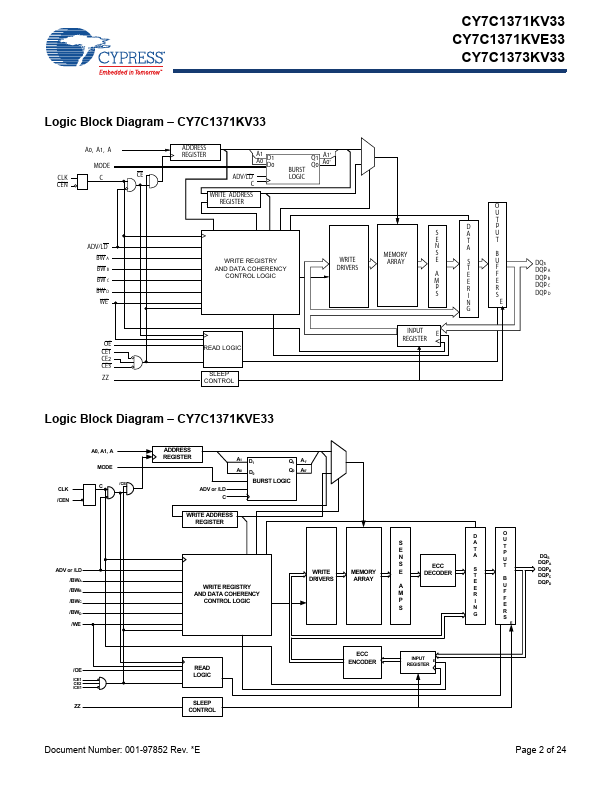
Datasheet4U Logo Datasheet4U.com

CY7C1371KVE33 - 18-Mbit (512K x 36/1M x 18) Flow-Through SRAM

Download the CY7C1371KVE33 datasheet PDF (CY7C1371KV33 included). The manufacturer datasheet provides complete specifications, pinout details, electrical characteristics, and typical applications for 18-mbit (512k x 36/1m x 18) flow-through sram.

Features

  • No Bus Latency (NoBL) architecture eliminates dead cycles between write and read cycles.
  • Supports up to 133-MHz bus operations with zero wait states.
  • Data is transferred on every clock.
  • Pin-compatible and functionally equivalent to ZBT™ devices.
  • Internally self-timed output buffer control to eliminate the need to use OE.
  • Registered inputs for flow through operation.
  • Byte write capability.
  • 3.3 V/2.5 V I/O power supply (VDDQ).
  • Fast clock-to-output ti.

📥 Download Datasheet

Note: The manufacturer provides a single datasheet file (CY7C1371KV33-CypressSemiconductor.pdf) that lists specifications for multiple related part numbers.
Other Datasheets by Cypress Semiconductor

Full PDF Text Transcription

Click to expand full text
CY7C1371KV33 CY7C1371KVE33 CY7C1373KV33 18-Mbit (512K × 36/1M × 18) Flow-Through SRAM with NoBL™ Architecture (With ECC) 18-Mbit (512K × 36/1M × 18) Flow-through SRAM with NoBL™ Architecture (With ECC) Features ■ No Bus Latency (NoBL) architecture eliminates dead cycles between write and read cycles ■ Supports up to 133-MHz bus operations with zero wait states ❐ Data is transferred on every clock ■ Pin-compatible and functionally equivalent to ZBT™ devices ■ Internally self-timed output buffer control to eliminate the need to use OE ■ Registered inputs for flow through operation ■ Byte write capability ■ 3.3 V/2.5 V I/O power supply (VDDQ) ■ Fast clock-to-output times ❐ 6.
Published: |