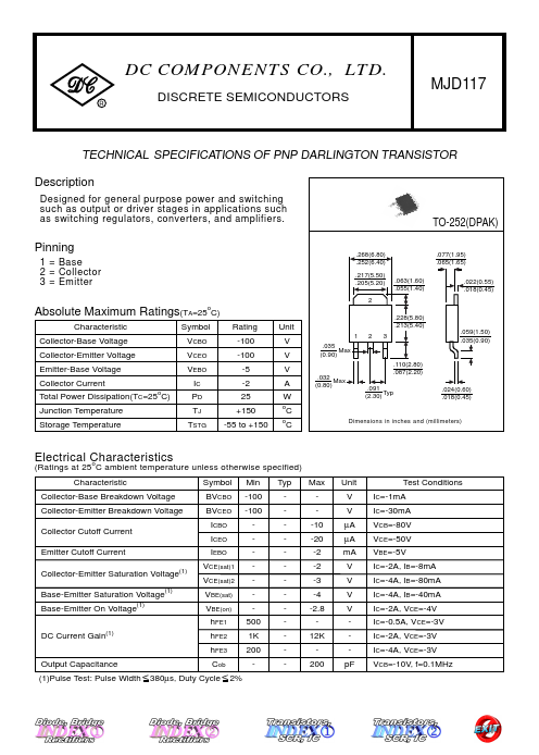
MJD117 Description
Designed for general purpose power and switching such as output or driver stages in applications such as switching regulators, converters, and amplifiers.
MJD117 is PNP DARLINGTON TRANSISTOR manufactured by DC COMPONENTS.
| Manufacturer | Part Number | Description |
|---|---|---|
| MJD117 | PNP Silicon Darlington Transistor | |
| MJD117 | Silicon PNP Power Transistor | |
| MJD117 | COMPLEMENTARY DARLINGTON PLASTIC POWER TRANSISTORS | |
| MJD117 | PNP Transistor | |
| MJD117 | Epitaxial Planar PNP Transistor |
Designed for general purpose power and switching such as output or driver stages in applications such as switching regulators, converters, and amplifiers.