Datasheet4U Logo Datasheet4U.com

EDD2508AKTA-5 - 256M bits DDR SDRAM (32M words x 8 bits DDR400)

Datasheet Summary

Description

The EDD2508AKTA-5 is a 256M bits DDR SDRAM organized as 8,388,608 words × 8 bits × 4 banks.

Read and write operations are performed at the cross points of the CK and the /CK.

This high-speed data transfer is realized by the 2 bits prefetch-pipelined architecture.

Features

  • Power supply: VDDQ = 2.6V ± 0.1V : VDD = 2.6V ± 0.1V.
  • Data rate: 400Mbps (max. ).
  • Double Data Rate architecture; two data transfers per clock cycle.
  • Bi-directional, data strobe (DQS) is transmitted /received with data, to be used in capturing data at the receiver.
  • Data inputs, outputs, and DM are synchronized with DQS.
  • 4 internal banks for concurrent operation.
  • DQS is edge aligned with data for READs; center aligned with data for WRI.

📥 Download Datasheet

Datasheet preview – EDD2508AKTA-5

Datasheet Details

Part number EDD2508AKTA-5
Manufacturer Elpida Memory
File Size 591.94 KB
Description 256M bits DDR SDRAM (32M words x 8 bits DDR400)
Datasheet download datasheet EDD2508AKTA-5 Datasheet
Additional preview pages of the EDD2508AKTA-5 datasheet.
Other Datasheets by Elpida Memory

Full PDF Text Transcription

Click to expand full text
( DataSheet : www.DataSheet4U.com ) PRELIMINARY DATA SHEET 256M bits DDR SDRAM EDD2508AKTA-5 (32M words × 8 bits, DDR400) Description The EDD2508AKTA-5 is a 256M bits DDR SDRAM organized as 8,388,608 words × 8 bits × 4 banks. Read and write operations are performed at the cross points of the CK and the /CK. This high-speed data transfer is realized by the 2 bits prefetch-pipelined architecture. Data strobe (DQS) both for read and write are available for high speed and reliable data bus design. By setting extended mode register, the on-chip Delay Locked Loop (DLL) can be set enable or disable. It is packaged in 66-pin plastic TSOP (II).
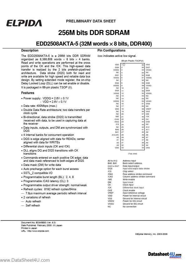
 Pin Configurations /xxx indicates active low signal.
Published: |