EDD5108ADTA-LI Overview
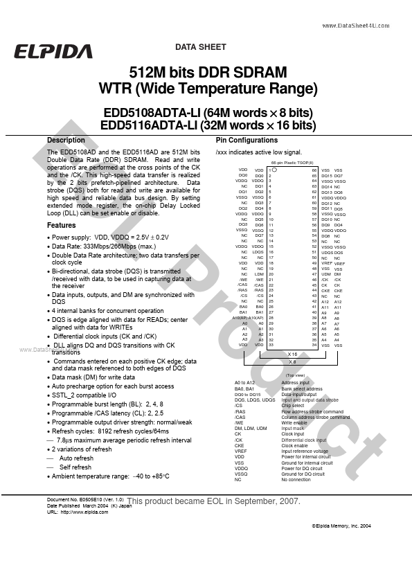
The EDD5108AD and the EDD5116AD are 512M bits Double Data Rate (DDR) SDRAM. Read and write operations are performed at the cross points of the CK and the /CK. This high-speed data transfer is realized by the 2 bits prefetch-pipelined architecture.
EDD5108ADTA-LI Key Features
- Power supply: VDD, VDDQ = 2.5V ± 0.2V
- Data Rate: 333Mbps/266Mbps (max.)
- Double Data Rate architecture; two data transfers per clock cycle
- Bi-directional, data strobe (DQS) is transmitted /received with data, to be used in capturing data at the receiver
- Data inputs, outputs, and DM are synchronized with DQS
- 4 internal banks for concurrent operation
- DQS is edge aligned with data for READs; center aligned with data for WRITEs
- Differential clock inputs (CK and /CK)
- DLL aligns DQ and DQS transitions with CK .. transitions
- mands entered on each positive CK edge; data and data mask referenced to both edges of DQS


