Datasheet4U Logo Datasheet4U.com

EDD5108ADTA - 512M bits DDR SDRAM

Description

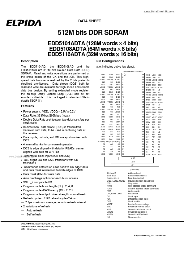
The EDD5104AD, the EDD5108AD and the EDD5116AD are 512M bits Double Data Rate (DDR) SDRAM.

Read and write operations are performed at the cross points of the CK and the /CK.

This highspeed data transfer is realized by the 2 bits prefetchpipelined architecture.

Features

  • Power supply: VDD, VDDQ = 2.5V ± 0.2V.
  • Data Rate: 333Mbps/266Mbps (max. ).
  • Double Data Rate architecture; two data transfers per clock cycle.
  • Bi-directional, data strobe (DQS) is transmitted /received with data, to be used in capturing data at the receiver.
  • Data inputs, outputs, and DM are synchronized with DQS.
  • 4 internal banks for concurrent operation.
  • DQS is edge aligned with data for READs; center aligned with data for WRITEs.

📥 Download Datasheet

Datasheet preview – EDD5108ADTA

Datasheet Details

Part number EDD5108ADTA
Manufacturer Elpida Memory
File Size 530.60 KB
Description 512M bits DDR SDRAM
Datasheet download datasheet EDD5108ADTA Datasheet
Additional preview pages of the EDD5108ADTA datasheet.
Other Datasheets by Elpida Memory

Full PDF Text Transcription

Click to expand full text
DATA SHEET 512M bits DDR SDRAM EDD5104ADTA (128M words × 4 bits) EDD5108ADTA (64M words × 8 bits) EDD5116ADTA (32M words × 16 bits) Description The EDD5104AD, the EDD5108AD and the EDD5116AD are 512M bits Double Data Rate (DDR) SDRAM. Read and write operations are performed at the cross points of the CK and the /CK. This highspeed data transfer is realized by the 2 bits prefetchpipelined architecture. Data strobe (DQS) both for read and write are available for high speed and reliable data bus design. By setting extended mode register, the on-chip Delay Locked Loop (DLL) can be set enable or disable. It is packaged in standard 66-pin plastic TSOP (II). Pin Configurations /xxx indicates active low signal.
Published: |