EDS5116ABTA
EDS5116ABTA is 512M bits SDRAM manufactured by Elpida Memory.
PRELIMINARY DATA SHEET
512M bits SDRAM
EDS5104ABTA (128M words × 4 bits) EDS5108ABTA (64M words × 8 bits) EDS5116ABTA (32M words × 16 bits)
Description
The EDS5104AB is a 512M bits SDRAM organized as 33,554,432 words × 4 bits × 4 banks. The EDS5108AB is a 512M bits SDRAM organized as 16,777,216 words × 8 bits × 4 banks. The EDS5116AB is a 512M bits SDRAM organized as 8,388,608 words × 16 bits × 4 banks. All inputs and outputs are referred to the rising edge of the clock input. It is packaged in standard 54pin plastic TSOP (II).
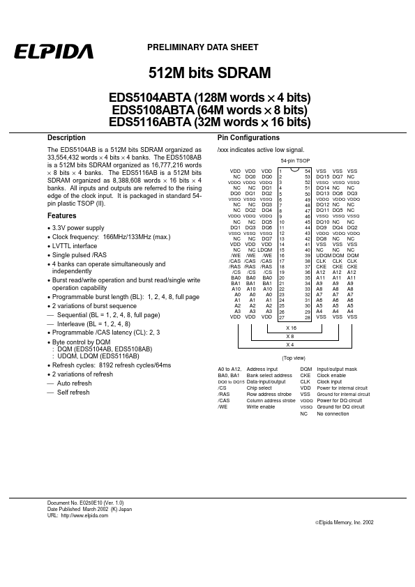
Pin Configurations
/xxx indicates active low signal.
54-pin TSOP VDD VDD NC DQ0 NC NC DQ0 DQ1 NC NC NC DQ2 NC NC DQ1 DQ3 NC VDD NC /WE /CAS /RAS /CS BA0 BA1 A10 A0 A1 A2 A3 VDD VDD DQ0 DQ1 DQ2 DQ3 DQ4 DQ5 DQ6
1 2 3 4 5 6 7 8 9 10 11 12 13 14 15 16 17 18 19 20 21 22 23 24 25 26 27 54 53 52 51 50 49 48 47 46 45 44 43 42 41 40 39 38 37 36 35 34 33 32 31 30 29 28
VSS VSS VSS DQ15 DQ7 NC
VSSQ VSSQ VSSQ
VDDQ VDDQ VDDQ
DQ14 NC NC DQ13 DQ6 DQ3
VDDQ VDDQ VDDQ
VSSQ VSSQ VSSQ
Features
- -
- -
- 3.3V power supply Clock frequency: 166MHz/133MHz (max.) LVTTL interface Single pulsed /RAS 4 banks can operate simultaneously and independently
- Burst read/write operation and burst read/single write operation capability
- Programmable burst length (BL): 1, 2, 4, 8, full page
- 2 variations of burst sequence Sequential (BL = 1, 2, 4, 8, full page) Interleave (BL = 1, 2, 4, 8)
- Programmable /CAS latency (CL): 2, 3
- Byte control by DQM : DQM (EDS5104AB, EDS5108AB) : UDQM, LDQM (EDS5116AB)
- Refresh cycles: 8192 refresh cycles/64ms
- 2 variations of refresh Auto refresh Self refresh
DQ12 NC NC DQ11 DQ5 NC
VSSQ VSSQ VSSQ
VDDQ VDDQ VDDQ
DQ10 NC NC DQ9 DQ4...