FDP14AN06LA0 Overview
Key Specifications
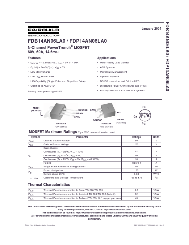
Package: TO-220AB
Mount Type: Through Hole
Pins: 3
Max Operating Temp: 175 °C
Key Features
- r DS(ON) = 12.8mΩ (Typ.), VGS = 5V, ID = 60A
- Qg(tot) = 24nC (Typ.), VGS = 5V
- Low Miller Charge
- Low QRR Body Diode
- UIS Capability (Single Pulse and Repetitive Pulse)
- Qualified to AEC Q101 Formerly developmental type 83557