• Part: MRFE6S9135HR3
  • Description: N-Channel Enhancement-Mode Lateral MOSFETs
  • Category: MOSFET
  • Manufacturer: Freescale Semiconductor
  • Size: 481.02 KB
Download MRFE6S9135HR3 Datasheet PDF
Freescale Semiconductor
MRFE6S9135HR3
MRFE6S9135HR3 is N-Channel Enhancement-Mode Lateral MOSFETs manufactured by Freescale Semiconductor.
Features - 100% PAR Tested for Guaranteed Output Power Capability - Characterized with Series Equivalent Large - Signal Impedance Parameters - Internally Matched for Ease of Use - Qualified Up to a Maximum of 32 VDD Operation - Integrated ESD Protection - Optimized for Doherty Applications - Ro HS pliant - 
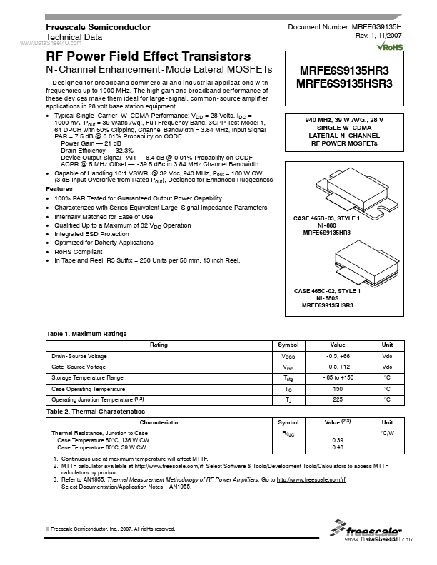
In Tape and Reel. R3 Suffix = 250 Units per 56 mm, 13 inch Reel. MRFE6S9135HR3 MRFE6S9135HSR3 940 MHz, 39 W AVG., 28 V SINGLE W - CDMA LATERAL N - CHANNEL RF POWER MOSFETs CASE 465B - 03, STYLE 1 NI - 880 MRFE6S9135HR3 CASE 465C - 02, STYLE 1 NI - 880S MRFE6S9135HSR3 Table 1. Maximum Ratings Rating Drain- Source Voltage Gate- Source Voltage Storage Temperature Range Case Operating Temperature Operating Junction Temperature (1,2) Symbol VDSS VGS Tstg TC TJ Value - 0.5, +66 - 0.5, +12 - 65 to +150 150 225 Unit Vdc Vdc °C °C °C Table 2. Thermal Characteristics Characteristic Thermal Resistance, Junction to Case Case Temperature 80°C, 136 W CW Case Temperature 80°C, 39 W CW Symbol RθJC Value (2,3) 0.39 0.48 Unit °C/W 1. Continuous use at maximum temperature will affect MTTF. 2. MTTF calculator available at http://.freescale./rf. Select Software & Tools/Development Tools/Calculators to access MTTF calculators by product. 3. Refer to AN1955, Thermal Measurement Methodology of RF Power Amplifiers. Go to http://.freescale./rf. Select Documentation/Application Notes - AN1955. © Freescale Semiconductor, Inc., 2007. All rights reserved. MRFE6S9135HR3 MRFE6S9135HSR3 1 RF Device Data Freescale Semiconductor Table 3. ESD Protection Characteristics .. Test Methodology Class II (Minimum) A (Minimum) IV (Minimum) Human Body Model (per JESD22 - A114) Machine Model (per EIA/JESD22 - A115) Charge Device Model (per JESD22 - C101) Table 4. Electrical Characteristics (TC = 25°C unless otherwise noted) Characteristic Off Characteristics Zero Gate Voltage Drain Leakage Current (VDS = 66 Vdc, VGS = 0 Vdc) Zero Gate Voltage Drain...