Datasheet4U Logo Datasheet4U.com

MW7IC18100GNR1 - RF LDMOS Wideband Integrated Power Amplifiers

Description

6.8 pF Chip Capacitors 10 μF, 50 V Chip Capacitors 0.2 pF Chip Capacitors 0.5 pF Chip Capacitors 0.8 pF Chip Capacitor 1.5 pF Chip Capacitor 2.2 μF, 16 V Chip Capacitor 470 μF, 63 V Electrolytic Capacitor, Radial 10 KΩ, 1/4 W Chip Resistors Part Number ATC100B6R8BT500XT GRM55DR61H106KA88L ATC100B0R2

Features

  • Characterized with Series Equivalent Large - Signal Impedance Parameters and Common Source Scattering Parameters.
  • On - Chip Matching (50 Ohm Input, DC Blocked).
  • Integrated Quiescent Current Temperature Compensation with Enable/Disable Function (1).
  • Integrated ESD Protection.
  • 200°C Capable Plastic Package.
  • RoHS Compliant.
  • In Tape and Reel. R1 Suffix = 500 Units per 44 mm, 13 inch Reel. MW7IC18100NR1 MW7IC18100GNR1 MW7IC18100NBR1 199.

📥 Download Datasheet

Other Datasheets by Freescale Semiconductor

Full PDF Text Transcription

Click to expand full text
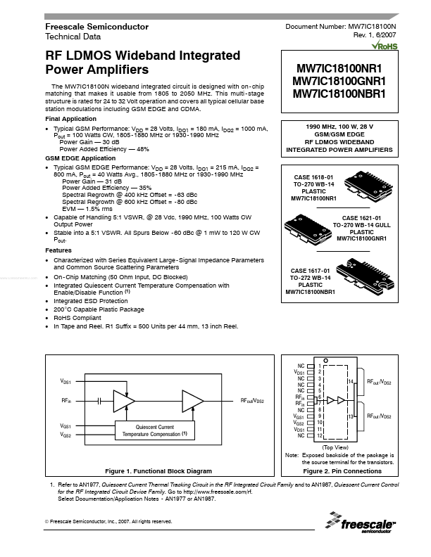
Freescale Semiconductor Technical Data Document Number: MW7IC18100N Rev. 1, 6/2007 RF LDMOS Wideband Integrated Power Amplifiers The MW7IC18100N wideband integrated circuit is designed with on - chip matching that makes it usable from 1805 to 2050 MHz. This multi - stage structure is rated for 24 to 32 Volt operation and covers all typical cellular base station modulations including GSM EDGE and CDMA. Final Application • Typical GSM Performance: VDD = 28 Volts, IDQ1 = 180 mA, IDQ2 = 1000 mA, Pout = 100 Watts CW, 1805 - 1880 MHz or 1930 - 1990 MHz Power Gain — 30 dB Power Added Efficiency — 48% GSM EDGE Application • Typical GSM EDGE Performance: VDD = 28 Volts, IDQ1 = 215 mA, IDQ2 = 800 mA, Pout = 40 Watts Avg.
Published: |